6502.org Forum  Projects  Code  Documents  Tools  Forum
It is currently Wed May 22, 2024 9:36 pm

All times are UTC


Post new topic Reply to topic  [ 16 posts ]  Go to page 1, 2  Next
Author Message
PostPosted: Fri Oct 28, 2022 9:13 pm 
Offline

Joined: Wed Oct 26, 2022 8:46 pm
Posts: 10
I know the max frequency is voltage dependant, but are the timings given in nanoseconds dependant on the voltage or frequency? Or is it more complex and depends on which specific timing I'm referring to?

The chart on page 25 of WDC's 6502 datasheet only gives timings between 5V (14 MHz max) to 1.8V (2 MHz max). I intend to use 5V at 1 MHz.

_________________
"To err is human, to really foul things up requires a computer!"
Tried to register with my legitimate email and never got the activation message. My spam-magnet email worked fine.

If you want to email me, please use neamerjell@gmail.com


Top
 Profile  
Reply with quote  
PostPosted: Fri Oct 28, 2022 9:17 pm 
Offline
User avatar

Joined: Thu Dec 11, 2008 1:28 pm
Posts: 10802
Location: England
I think most of the times are absolute, varying with voltage. The only exceptions I'd expect would be minimum cycle times, which of course define the frequency. But I haven't looked carefully at the table.


Top
 Profile  
Reply with quote  
PostPosted: Fri Oct 28, 2022 9:35 pm 
Offline
User avatar

Joined: Thu May 28, 2009 9:46 pm
Posts: 8191
Location: Midwestern USA
MiraLagatta wrote:
I know the max frequency is voltage dependant, but are the timings given in nanoseconds dependant on the voltage or frequency? Or is it more complex and depends on which specific timing I'm referring to?

The chart on page 25 of WDC's 6502 datasheet only gives timings between 5V (14 MHz max) to 1.8V (2 MHz max). I intend to use 5V at 1 MHz.

On paper, the higher the voltage, the lower the propagation time through a CMOS device. This characteristic implies that timing is dependent on voltage—higher voltage yields faster operation. Of course, there is a voltage ceiling, beyond which the device will be damaged.

Some of WDC’s timing values don’t make a whole lot of sense when viewed in the context of the “F Max vs Vdd” curve published on page 24 in the 65C02 data sheet. You can take some solace in the fact that their 65C02 can be run a lot faster than the timing chart suggests. Plasmo has gotten his CRC65 unit running at 29 MHz, if I correctly recall.

_________________
x86?  We ain't got no x86.  We don't NEED no stinking x86!


Top
 Profile  
Reply with quote  
PostPosted: Fri Oct 28, 2022 9:51 pm 
Offline

Joined: Wed Oct 26, 2022 8:46 pm
Posts: 10
Thanks again BDDinosaur! Based on both responses, I believe I should refer to the 5V (14MHz max) column since that is the voltage I intend to use. This goes a long way towards furthering my understanding of the timing diagram and the animated timing diagram that was linked in Garth's primer.

_________________
"To err is human, to really foul things up requires a computer!"
Tried to register with my legitimate email and never got the activation message. My spam-magnet email worked fine.

If you want to email me, please use neamerjell@gmail.com


Top
 Profile  
Reply with quote  
PostPosted: Fri Oct 28, 2022 10:00 pm 
Offline
User avatar

Joined: Thu May 28, 2009 9:46 pm
Posts: 8191
Location: Midwestern USA
MiraLagatta wrote:
Thanks again BDDinosaur! Based on both responses, I believe I should refer to the 5V (14MHz max) column since that is the voltage I intend to use. This goes a long way towards furthering my understanding of the timing diagram and the animated timing diagram that was linked in Garth's primer.

Be economical with your use of gates in your glue logic and you likely will have no timing worries. As you increase address decoding granularity, you are forced to cascade more gates and prop time can quickly get out of hand.

_________________
x86?  We ain't got no x86.  We don't NEED no stinking x86!


Top
 Profile  
Reply with quote  
PostPosted: Sat Oct 29, 2022 7:52 am 
Offline

Joined: Wed Oct 26, 2022 8:46 pm
Posts: 10
This question arose mostly due to me second guessing what I thought I already knew. Its good to have confirmation that I was on the right track. Thanks to BDDinosaur and Garth Wilson, I have a much better understanding of what I'm looking at in the datasheets.

Now, I'm confident that I can crunch numbers this weekend and make sure the timings on everything I plan to use is going to work. I'm not blindly copying anyone else's working design because I want to actually understand how and why it does what it does.

The idea I have at the moment is to "borrow" a memory map from elsewhere on this forum (I forget who posted it):

0000-7FFF 32K RAM (eventually, I want to load programs from an SD card)
8000-83FF 1K I/O (far more than I think I will need, famous last words...)
8400-FFFF 31K ROM (would basically function like a BIOS in a modern PC, handles keyboard, 128x64 LCD, SD card)

I think I figured out how to achieve this:
74HC00 Quad NAND gate
( NOT(A15) NAND CLK ) = RAM_CS\

74HC682 { Inputs 2 bytes, outputs P=Q or P>Q }
A15-A10 connected to P, lowest 2 bits of P tied to ground
10000000 hard wired to Q
P=Q = I/O_CS\
P>Q = ROM_CS\

Primary goal: Get it working and understand it well enough to successfully explain it to someone else.
Secondary goal: Have the ability to write and compile programs on my PC, transfer them to an SDcard (just copy it in Windows explorer, not make a disk image), then load and run them on my 6502 computer - this will most likely involve using an Arduino to handle the FAT32 file system.
Long term goal: Port BASIC to my 6502 computer.

Ambitious, I know, but I think I'm up to the task.

_________________
"To err is human, to really foul things up requires a computer!"
Tried to register with my legitimate email and never got the activation message. My spam-magnet email worked fine.

If you want to email me, please use neamerjell@gmail.com


Top
 Profile  
Reply with quote  
PostPosted: Sat Oct 29, 2022 12:28 pm 
Offline

Joined: Fri Jul 09, 2021 10:12 pm
Posts: 741
MiraLagatta wrote:
Primary goal: Get it working and understand it well enough to successfully explain it to someone else.
Secondary goal: Have the ability to write and compile programs on my PC, transfer them to an SDcard (just copy it in Windows explorer, not make a disk image), then load and run them on my 6502 computer - this will most likely involve using an Arduino to handle the FAT32 file system.
Long term goal: Port BASIC to my 6502 computer.

Ambitious, I know, but I think I'm up to the task.

Nice goals, good luck with them! Reading FAT32 from SD cards is not out of the question even without an Arduino in between - if you're happy to borrow code, I shared a fairly compact implementation on github a few years ago, and have been using it pretty much unchanged since then, especially for large data files.
You can see it here if you like: https://github.com/gfoot/sdcard6502/blo ... Library.md


Top
 Profile  
Reply with quote  
PostPosted: Sat Oct 29, 2022 4:00 pm 
Offline

Joined: Wed Oct 26, 2022 8:46 pm
Posts: 10
Quote:
Reading FAT32 from SD cards is not out of the question even without an Arduino in between - if you're happy to borrow code, I shared a fairly compact implementation on github a few years ago, and have been using it pretty much unchanged since then, especially for large data files.
You can see it here if you like: https://github.com/gfoot/sdcard6502/blo ... Library.md


Gfoot, your writeup on the SD card, which I found through HackaDay, is what gave me the idea to use one in my project!

I'd be happy to borrow your code, and of course give you credit, but I gotta understand it first. One thing at a time. The main reason it's taken nearly a year from buying the kit to put anything on a breadboard is all the research I've been doing. In order to understand this, I need to understand that, but before I can, I need to know how this other thing works... six rabbit holes later, it's 3am and my brain is fried. LOL! I'm sure everyone in this forum has been there, done that at some point. Thanks for the good luck wish, I'm going to need it!

_________________
"To err is human, to really foul things up requires a computer!"
Tried to register with my legitimate email and never got the activation message. My spam-magnet email worked fine.

If you want to email me, please use neamerjell@gmail.com


Top
 Profile  
Reply with quote  
PostPosted: Sat Oct 29, 2022 6:44 pm 
Offline
User avatar

Joined: Thu May 28, 2009 9:46 pm
Posts: 8191
Location: Midwestern USA
MiraLagatta wrote:
The idea I have at the moment is to "borrow" a memory map from elsewhere on this forum (I forget who posted it):

0000-7FFF 32K RAM (eventually, I want to load programs from an SD card)
8000-83FF 1K I/O (far more than I think I will need, famous last words...)
8400-FFFF 31K ROM (would basically function like a BIOS in a modern PC, handles keyboard, 128x64 LCD, SD card)

I think I figured out how to achieve this:
74HC00 Quad NAND gate
( NOT(A15) NAND CLK ) = RAM_CS\...

For the benefit of your readers, your glue logic would be easier to visualize in schematic form. You can attach a schematic in a PDF or as a graphic, e.g., GIF or JPEG. It’s the old “One picture is worth a 1000 words.” thingie...

_________________
x86?  We ain't got no x86.  We don't NEED no stinking x86!


Top
 Profile  
Reply with quote  
PostPosted: Sat Oct 29, 2022 11:18 pm 
Offline

Joined: Wed Oct 26, 2022 8:46 pm
Posts: 10
Quote:
For the benefit of your readers, your glue logic would be easier to visualize in schematic form.


[s]Will do, once I get it drawn up.[/s]

BTW: if a picture is worth 1,000 words, is a video worth 60,000 words per second? :P

Here is my proposed address decoder:
Attachment:
File comment: My Address Decoder
My Address Decoder - BW.png
My Address Decoder - BW.png [ 46.74 KiB | Viewed 823 times ]


Also, the datasheet for my RAM has this note about the write operation:
Quote:
9. If CS goes low simultaneously with WE going low or after WE going low, the outputs remain in the high impedance state.


I initially thought this means that if R/W somehow wins the race and goes low before or at the same time as CE, that the write operation won't work, but Ben Eater built his computer with R/W going straight to WE seemingly without any issues. So, what does this actually mean?

Timing diagram it refers to:
Attachment:
File comment: RAM Write Timing Diagram
RAM Write Timing Diagram - Unmodified.png
RAM Write Timing Diagram - Unmodified.png [ 245.44 KiB | Viewed 818 times ]

_________________
"To err is human, to really foul things up requires a computer!"
Tried to register with my legitimate email and never got the activation message. My spam-magnet email worked fine.

If you want to email me, please use neamerjell@gmail.com


Top
 Profile  
Reply with quote  
PostPosted: Sun Oct 30, 2022 5:56 am 
Offline
User avatar

Joined: Thu May 28, 2009 9:46 pm
Posts: 8191
Location: Midwestern USA
MiraLagatta wrote:
Here is my proposed address decoder...

Well, it won’t be very speedy. :D

Quote:
Also, the datasheet for my RAM has this note about the write operation:

    9. If CS goes low simultaneously with WE going low or after WE going low, the outputs remain in the high impedance state.

I initially thought this means that if R/W somehow wins the race and goes low before or at the same time as CE, that the write operation won't work, but Ben Eater built his computer with R/W going straight to WE seemingly without any issues. So, what does this actually mean?

It depends on the SRAM you’re using. Some are fussy about the order in which the control inputs are asserted and others are not.

In my POC unit, I use an ISSI 128KB SRAM, whose data sheet doesn’t give any exact description of what will happen if /CE is asserted after /OE or /WE has been asserted. However, the timing diagrams indicate that response to /OE or /WE is faster if preceded by chip select. Ergo the technique of gating chip select with Ø2 will slow the device’s response, especially if /CE is continuously asserted, as I’ve seen in some circuits.

Bottom line, best performance will be seen by not using Ø2 to qualify chip selects. This will be especially important as you work toward higher clock speeds, since you are already on the path to a lot of prop delay in your glue logic. Instead, qualify /WE with Ø2 in a 65C02 system, and also qualify /OE with Ø2 in a 65C816 system. Qualifying /OE with Ø2 in a 65C02 system is optional, but won't hurt performance if done right.

By the way, all control inputs to 65xx devices (6520, 6522, etc.) must be stable prior to the rise of Ø2. These devices will not operate if you gate any of their control signals (RWB, CS1, etc.) with Ø2.

_________________
x86?  We ain't got no x86.  We don't NEED no stinking x86!


Top
 Profile  
Reply with quote  
PostPosted: Sun Oct 30, 2022 7:21 am 
Online
User avatar

Joined: Fri Aug 30, 2002 1:09 am
Posts: 8442
Location: Southern California
MiraLagatta wrote:
Also, the datasheet for my RAM has this note about the write operation:
Quote:
9. If CS goes low simultaneously with WE going low or after WE going low, the outputs remain in the high impedance state.

I initially thought this means that if R/W somehow wins the race and goes low before or at the same time as CE, that the write operation won't work, but Ben Eater built his computer with R/W going straight to WE seemingly without any issues. So, what does this actually mean?

Timing diagram it refers to:
Attachment:
RAM Write Timing Diagram - Unmodified.png

It's not a race; it just means that while both WE\ and CS\ are low, the outputs won't be enabled, regardless of the state of OE\. If you do have OE\ low, and then take CS\ low before WE\, there will be that short time that it tries to put something on the bus, and there will be that short time of bus contention if the processor is also driving it, whether either one has arrived at a valid value to drive or not. Note that there's no txx specification for a relationship between CS\ and WE\, or between CS\ and OE\, or between OE\ and WE\.

BigDumbDinosaur wrote:
Well, it won’t be very speedy. :D

That was my first thought when he said he wanted to use a 74HC682; but I had to remind myself he said "I intend to use 5V at 1 MHz."

MiraLagatta wrote:
The chart on page 25 of WDC's 6502 datasheet only gives timings between 5V (14 MHz max) to 1.8V (2 MHz max).

MiraLagatta, keep in mind that the timing specifications are guarantees that it won't be any worse than that. The number of nanoseconds guaranteed to be the maximum remain, as Ed said, whether you run it at 14MHz, 1MHz, or .000000001 Hz. (Yes, on WDC's processors, you can stop the clock, in either phase, without their forgetting where they are and what they're supposed to do next.) WDC's data sheets have had an awful lot of errors over the years; but fortunately the parts can usually perform far, far better than guaranteed. BDD mentioned that forum member "plasmo" has gotten one running at 29MHz. Later, plasmo got one running at 40MHz @5.3V, 36MHz @ 5V. (See the edit at the end of viewtopic.php?p=85784#p85784 .)

_________________
http://WilsonMinesCo.com/ lots of 6502 resources
The "second front page" is http://wilsonminesco.com/links.html .
What's an additional VIA among friends, anyhow?


Top
 Profile  
Reply with quote  
PostPosted: Sun Oct 30, 2022 7:32 am 
Offline
User avatar

Joined: Thu Dec 11, 2008 1:28 pm
Posts: 10802
Location: England
Indeed, as the target speed is 1MHz, it's not fair to criticise that the design won't go at great speeds. It's not meant to, and the comment is just a temptation to scope creep.

Keep it simple, stick to your goals, and get it working. Plenty of possibilities for going further, after you have something working.


Top
 Profile  
Reply with quote  
PostPosted: Mon Oct 31, 2022 5:01 am 
Offline

Joined: Wed Oct 26, 2022 8:46 pm
Posts: 10
BigEd wrote:
Indeed, as the target speed is 1MHz, it's not fair to criticise that the design won't go at great speeds. It's not meant to, and the comment is just a temptation to scope creep.

Keep it simple, stick to your goals, and get it working. Plenty of possibilities for going further, after you have something working.


Exactly! I want to build a computer that I can understand, not brag about how fast it goes, although I may brag that I understand every last bit of how it works (once I do)... :P

When I got my first PC, I wondered how it "knew" where to look for DOS. Just a couple years ago, I installed Arch Linux on a computer - by hand "the Arch way", no fancy automated installers. I learned the BIOS is hard coded to look in the first 512 bytes of whatever storage is available. Now, after researching the 6502, I'm assuming modern CPUs also have reset vectors or equivalent that are hard wired and tell them where to look for the BIOS startup routine.

As I stated before, one of my goals is to mimic an old pre-Pentium era PC design (386, 486), using the ROM as a sort of BIOS, which loads programs from some sort of mass storage, most likely an SD card.

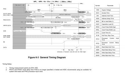
I rewatched Ben Eater's bus timing video https://www.youtube.com/watch?v=i_wrxBdXTgM&ab_channel=BenEater again and this time I stopped it multiple times to make notes on my own timing diagram, similar to how he did it. Even he admits that the 6502's timing diagram is a bit convoluted. I grabbed a screenshot of the PDF, threw it into Paint.Net (Photoshop for poor people), added the nanosecond timings directly to the diagram, and added the definitions of the abbreviations along the side and footnotes on the bottom. Everything is on one page and I don't have to flip back and forth between two or three pages any more.

Attachment:
6502 Timing Diagram -BW.png
6502 Timing Diagram -BW.png [ 729.8 KiB | Viewed 751 times ]


This went a long way towards fully understanding what I was looking at! It also put in plain view why chip select is tied to the high end of the clock cycle.

_________________
"To err is human, to really foul things up requires a computer!"
Tried to register with my legitimate email and never got the activation message. My spam-magnet email worked fine.

If you want to email me, please use neamerjell@gmail.com


Top
 Profile  
Reply with quote  
PostPosted: Mon Oct 31, 2022 8:14 am 
Offline
User avatar

Joined: Thu Dec 11, 2008 1:28 pm
Posts: 10802
Location: England
One thing I quite like to try to make clear, although it verges on the pedantic, is that for almost all purposes the rising edge of the clock is not a timing reference. It's a very convenient point in the cycle and it's very often used, in effect, to qualify some control signals to arrange that the design is safe and correct. However, it is just a point in the cycle, and if a design had another timing reference which falls neither too early nor too late then it would do just as well.

In your diagram - which is a great idea - we see just two signals referred to the rising edge. One is the rarely-used input SOB. The other is the validity of the databus during a write cycle. As that's not a control signal, there's no safety aspect there for normal designs - the constraint of interest is the receiving device's need to see stable data, which will normally be measured as a setup time, in advance of the falling edge.

As I say, a slightly pedantic point. But I think it helps to have a correct view of what causes what, as well as when things happen.


Top
 Profile  
Reply with quote  
Display posts from previous:  Sort by  
Post new topic Reply to topic  [ 16 posts ]  Go to page 1, 2  Next

All times are UTC


Who is online

Users browsing this forum: No registered users and 2 guests


You cannot post new topics in this forum
You cannot reply to topics in this forum
You cannot edit your posts in this forum
You cannot delete your posts in this forum
You cannot post attachments in this forum

Search for:
Jump to: