Externalized Wishbone Bus Design
-
GARTHWILSON

- Forum Moderator
- Posts: 8773
- Joined: 30 Aug 2002
- Location: Southern California
- Contact:
Re: Externalized Wishbone Bus Design
I like the distributed grounds. +5V bypassed to ground would qualify for purposes of good AC performance too. As far as routing the 96-pin connector goes, there's no problem getting two traces per layer between pins of row C (the row farthest from the edge of the board); so I don't think you need to worry about having any difficulty at all routing the 96-pin. You might even be able to get three traces between pins; but it won't be necessary. I think every board house around will do .006"/.006" trace/space before charging extra. Some can make the trace as narrow as its thickness, so it has a square cross section. How they can do that is beyond me, but I've seen photomicrographs of it. You can also get WW 96-pin DINs (which I'm using).
http://WilsonMinesCo.com/ lots of 6502 resources
The "second front page" is http://wilsonminesco.com/links.html .
What's an additional VIA among friends, anyhow?
The "second front page" is http://wilsonminesco.com/links.html .
What's an additional VIA among friends, anyhow?
Re: Externalized Wishbone Bus Design
My PCB layout software complained of DRC violations when I tried putting two traces between row C pads. Maybe there is a setting I can tweak, or maybe the footprint uses pads which are bigger than what you use.
-
GARTHWILSON
- Forum Moderator
- Posts: 8773
- Joined: 30 Aug 2002
- Location: Southern California
- Contact:
Re: Externalized Wishbone Bus Design
For most things, I use pads that are only .020" greater diameter than the finished hole. So for example thru-hole ICs' pads are usually .050" diameter with .030" hole, leaving .050" between pads which allows getting two traces in between pads using .010" trace and space, or three three traces in between pads if minimum trace & space are .006" or .007". For .025" square posts (like pin headers), I use a .040" hole and .060" pad, leaving .040" in between, which still allows two traces through if minimum trace and space is .008" or less. I'm always watching the X-Y display, frequently use the calculator to get things spaced right rather than rely on eyeballing something, and I don't use snap-to-grid (unless .001" is considered a grid).
http://WilsonMinesCo.com/ lots of 6502 resources
The "second front page" is http://wilsonminesco.com/links.html .
What's an additional VIA among friends, anyhow?
The "second front page" is http://wilsonminesco.com/links.html .
What's an additional VIA among friends, anyhow?
Re: Externalized Wishbone Bus Design
Well, thanks to the advice from Garth on how to pack things in between the pins of the DIN connector, I finally ended up with a PCB layout like so: 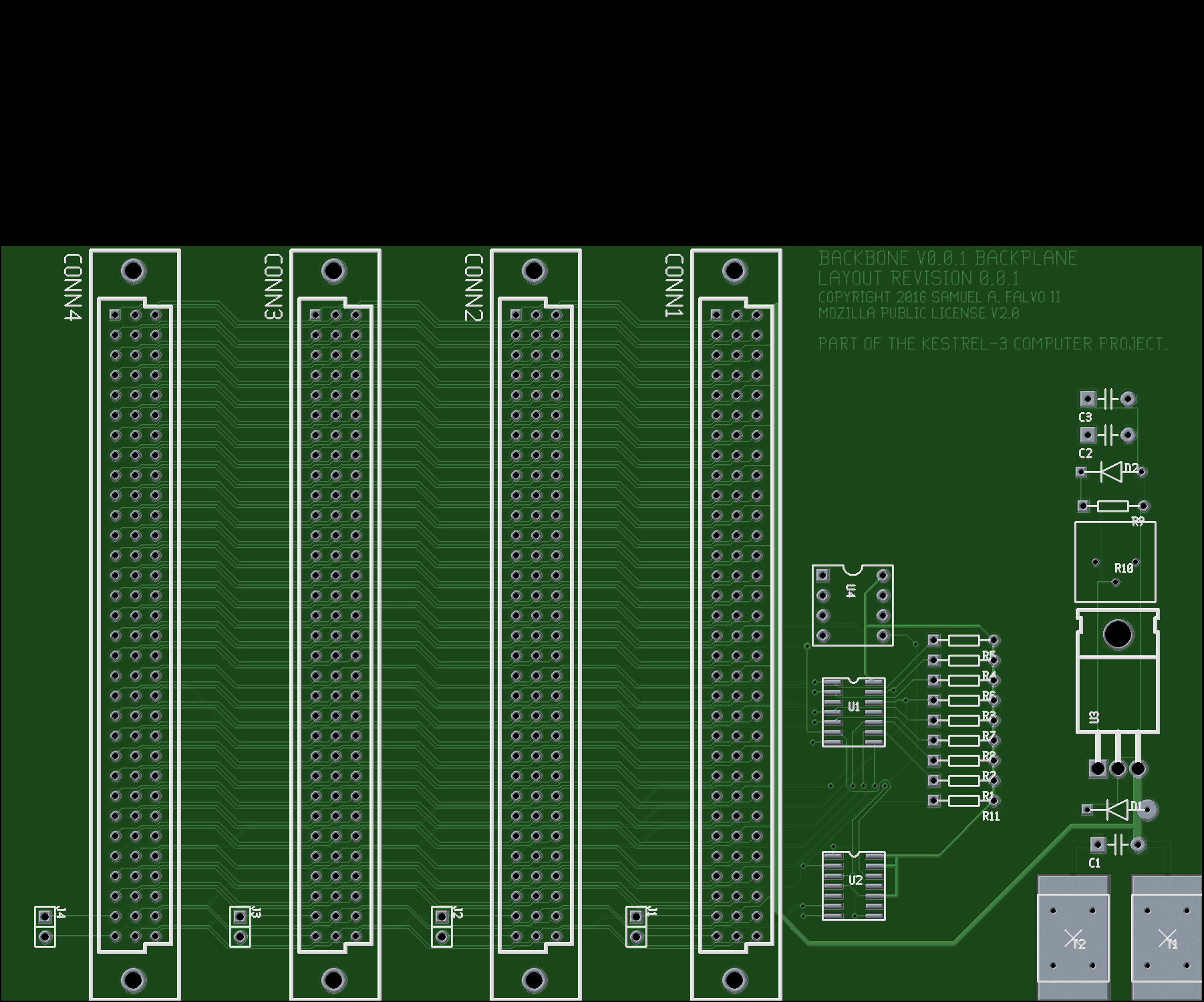
This is, of course, just a preview of what the finished board would look like. The reverse side is boring: just a grounded copper fill with a few necessary traces to avoid jumpers on the top-side.
The power supply section is in need of manual rework; I think some of the traces are too small. Not that it matters for my immediate needs (I'm just driving two LV-TTL chips), but I think some of those traces should be thickened and re-routed by hand. It's the only section that I used auto-routing on, and that was only to clean up the display while I hand-routed the DIN connectors and TTL logic.

Re: Externalized Wishbone Bus Design
Hi Sam -- nice PCB!  Reminder, though: It's a bit easier (and better) if you attach images to your posts, rather than hosting 'em off-site.
Hmm, maybe you already noticed, but it seems that, for the final version, those zig-zags could advantageously be moved a bit -- horizontally I mean. (Original and modified motifs shown below.) It's just a suggestion; I realize the Design Rules may be satisfied as-is.
Is the back side intended to act as a ground plane, then? Connector pins that're grounded attach to it? (Just asking. I hope those traces you mentioned are short.)
cheers
Jeff
kc5tja wrote:
Well, thanks to the advice from Garth on how to pack things in between the pins of the DIN connector, I finally ended up with a PCB layout like so: [...] This is, of course, just a preview of what the finished board would look like.
kc5tja wrote:
The reverse side is boring: just a grounded copper fill with a few necessary traces to avoid jumpers on the top-side.
cheers
Jeff
In 1988 my 65C02 got six new registers and 44 new full-speed instructions!
https://laughtonelectronics.com/Arcana/ ... mmary.html
https://laughtonelectronics.com/Arcana/ ... mmary.html
-
GARTHWILSON
- Forum Moderator
- Posts: 8773
- Joined: 30 Aug 2002
- Location: Southern California
- Contact:
Re: Externalized Wishbone Bus Design
Yes, I started writing Thursday night, then put it aside, thinking what I wrote sounded too picky. I'm sure it'll work as is, and it does look nice so don't let this come across as negative.
_________________
Wow, it sure looks like you already got boards made; but how could it be so fast? It looks nice.
If that's just a super good simulated picture and they're not made yet, I'd say you could further improve the spacing between traces and pads by removing the lock to 45-degree increments so you can use any angle, then come out of every row-A and row-C pin away from the connector at nearly 0 degrees instead of 45, and making the traces spaced more equidistant rather than grouped in threes. If the rise times are fast enough to matter, you'll get less cross-coupling between traces if their separation, relative to the distance to the ground plane (which in this case is the thickness of the board), is increased.
Related, for my next picky point, I notice in Jeff's second picture that the traces come to pads with angles of less than 90 degrees. I would make it so the last segment of each trace heads straight for the center of the pad. PCB manufacture seems to have improved enough over the years that it may not be a problem anymore, but the smaller angles tended to be harder to wash the chemicals out of in the manufacturing process, leading to problems in long-term reliability. I still try to have no angles of less than 90 degrees.
http://WilsonMinesCo.com/ lots of 6502 resources
The "second front page" is http://wilsonminesco.com/links.html .
What's an additional VIA among friends, anyhow?
The "second front page" is http://wilsonminesco.com/links.html .
What's an additional VIA among friends, anyhow?
Re: Externalized Wishbone Bus Design
GARTHWILSON wrote:
Wow, it sure looks like you already got boards made; but how could it be so fast? It looks nice.
Quote:
If that's just a super good simulated picture and they're not made yet, I'd say you could further improve the spacing between traces and pads by removing the lock to 45-degree increments so you can use any angle, then come out of every row-A and row-C pin away from the connector at nearly 0 degrees instead of 45, and making the traces spaced more equidistant rather than grouped in threes.
That said, the center trace is either ground or +5V, and the reverse side is a ground plane, so I'm hoping that will compensate for this design.
Quote:
If the rise times are fast enough to matter
-
GARTHWILSON
- Forum Moderator
- Posts: 8773
- Joined: 30 Aug 2002
- Location: Southern California
- Contact:
Re: Externalized Wishbone Bus Design
I'd like to do a layout to illustrate what I mean, but don't wait for me. It may be a while before I can get to it. I still need to do some tests on undocumented '816 behavior details for one of our newest members too, since I have my tester set up and offered.
I believe the standard panels for 3U boards for a VME card cage are made for the slots to be 0.800" on centers. If that's of any interest to you, it might be good to space yours accordingly. You don't have to use panels, or use stock panel blanks.
I believe the standard panels for 3U boards for a VME card cage are made for the slots to be 0.800" on centers. If that's of any interest to you, it might be good to space yours accordingly. You don't have to use panels, or use stock panel blanks.
- NIcardcage.jpg (37.2 KiB) Viewed 4487 times
http://WilsonMinesCo.com/ lots of 6502 resources
The "second front page" is http://wilsonminesco.com/links.html .
What's an additional VIA among friends, anyhow?
The "second front page" is http://wilsonminesco.com/links.html .
What's an additional VIA among friends, anyhow?
Re: Externalized Wishbone Bus Design
My slots are spaced at 1.0" centers for easier access to the bus-grant jumpers and perhaps for sticking o'scope probes inside.
This backplane is not intended to sit in a rack, nor is it VME compatible. Its purpose is to let me break the Kestrel-3 into different components, so I can work on them in isolation. Once everything is done (where done is defined as, "I have a working computer with working video display and keyboard input"), I'd like to place everything onto a single board.
Is there a reason for recommending 0.8" centers, other than compatibility with existing card cage chassis?
-
GARTHWILSON
- Forum Moderator
- Posts: 8773
- Joined: 30 Aug 2002
- Location: Southern California
- Contact:
Re: Externalized Wishbone Bus Design
kc5tja wrote:
Is there a reason for recommending 0.8" centers, other than compatibility with existing card cage chassis?
Here's the portable rack, standing on end, looking at the bottom. The perforated top and bottom panels come out. The card guides snap in and out easily. The front panel will hold the LCD and keypad. It is on hinges, and is held down with thumbscrews during transport to protect things.
http://WilsonMinesCo.com/ lots of 6502 resources
The "second front page" is http://wilsonminesco.com/links.html .
What's an additional VIA among friends, anyhow?
The "second front page" is http://wilsonminesco.com/links.html .
What's an additional VIA among friends, anyhow?
Re: Externalized Wishbone Bus Design
Putting the slots at 1.6" centers would roughly double the cost of the board (doubles the surface area), and would lead to traces >4", thus requiring termination (instead of it being merely a recommendation). Also, card cages seem to be optimized for 100mm x 160mm Eurocards. I'm looking "cards" that are closer to 3.5" x 1.5" in size (give or take space needed for external ports). Again, looking to RC2014 computer for inspiration. The backplane is intended to carry the main CPU bus.
Re: Externalized Wishbone Bus Design
Fixed last known batch of bugs in the PCB layout, and I've now placed an order. Here's hoping everything works when I put it all together.
-
GARTHWILSON
- Forum Moderator
- Posts: 8773
- Joined: 30 Aug 2002
- Location: Southern California
- Contact:
Re: Externalized Wishbone Bus Design
We were talking about diode terminations on page 1 of this topic. I came across this ap. note from what used to be National Semiconductor (then Fairchild, now ON Semiconductor), regarding taking advantage of the static-protection diodes that are built into most CMOS ICs: https://www.onsemi.com/pub/Collateral/AN-610-D.PDF, "Terminations for Advanced CMOS Logic." It says in the first part under the "No Termination" heading,
In their note 393 at https://www.onsemi.com/pub/Collateral/AN-393-D.PDF, "Transmission-Line Effects Influence High-Speed CMOS," it says in the 3rd paragraph,
and later on,
- Clamp diodes at the inputs of most logic devices tend to reduce the ringing and over-shoots. Often, these clamp diodes are sufficient to insure reliable system operation.
In their note 393 at https://www.onsemi.com/pub/Collateral/AN-393-D.PDF, "Transmission-Line Effects Influence High-Speed CMOS," it says in the 3rd paragraph,
- Furthermore, controlling unwanted reflections is easier in the CMOS designs, because 54HC/74HC devices’ electrostatic-protection diodes tend to clamp the reflected voltages to the power-supply levels.
and later on,
- Also, the input of a 54HC/74HC gates has diodes to Vcc and ground; these diodes clamp the reflected signal as it tries to exceed the supply level.
http://WilsonMinesCo.com/ lots of 6502 resources
The "second front page" is http://wilsonminesco.com/links.html .
What's an additional VIA among friends, anyhow?
The "second front page" is http://wilsonminesco.com/links.html .
What's an additional VIA among friends, anyhow?