Overview:
6502.org wrote:
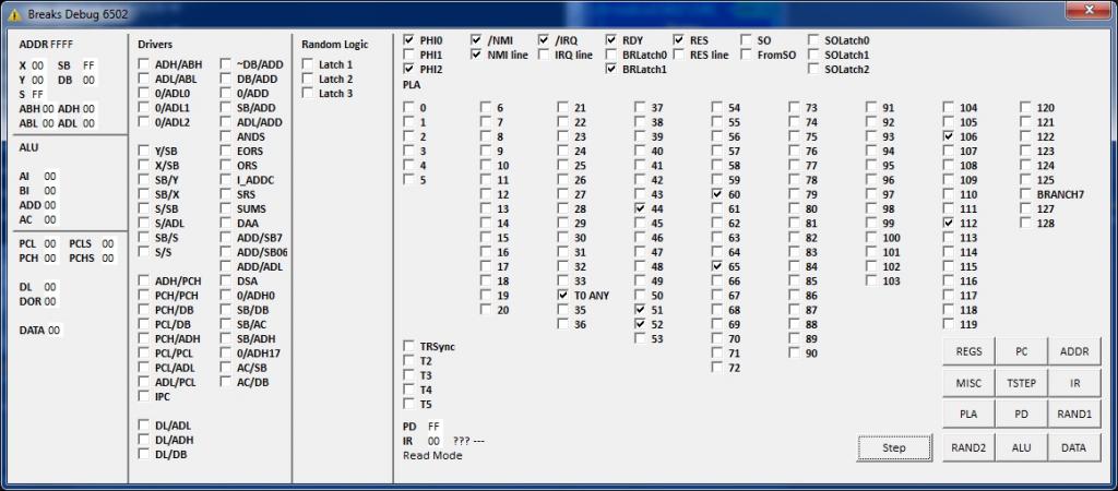
Image no longer available: http://ogamespec.com/imgstore/whc506de23b60f71.jpg
Code: Select all
        b = NOR ( NAND(NOT(NMI_PAD), PHI2), NMI_LATCH);
        NMI_LATCH = NOR ( NAND(NMI_PAD, PHI2), b );
        OUTPUT_LINE = NOT(NMI_LATCH);
I drawn NAND/NOR counterpart of trigger on picture. So I think we need those "~".
As output I'm getting following data:
Code: Select all
L N Ф  L*O
0 0 0 | 0 1
0 0 1 | 0 1
0 1 0 | 0 1
0 1 1 | 1 0
1 0 0 | 0 1
1 0 1 | 0 1
1 1 0 | 0 1
1 1 1 | 1 0
L - latch value before iteration
N - NMI pin level
Ф - PHI2
L* - latch value after iteration
O - output line
And it even worse, if you try to simulate /IRQ. It has additional PHI1 transfer gate + latch as output. In that case I'm getting only '1's on out.