6502.org Forum  Projects  Code  Documents  Tools  Forum
It is currently Sat Nov 23, 2024 11:26 am

All times are UTC


Post new topic Reply to topic  [ 86 posts ]  Go to page Previous  1, 2, 3, 4, 5, 6  Next
Author Message
PostPosted: Mon Aug 30, 2021 2:38 pm 
Offline
User avatar

Joined: Thu May 28, 2009 9:46 pm
Posts: 8509
Location: Midwestern USA
floobydust wrote:
Ouch! That hurts.... more fancy coasters for the workshop it seems.

Also, their straight edges make them good for drawing short lines. :shock:

J64C wrote:
Gotta post pics of the boards anyway though! Can’t leave us hanging. 8)

I suppose. I'll see what I can do.

_________________
x86?  We ain't got no x86.  We don't NEED no stinking x86!


Top
 Profile  
Reply with quote  
PostPosted: Tue Aug 31, 2021 2:19 am 
Offline

Joined: Sat Dec 30, 2017 3:19 pm
Posts: 116
Location: Detroit, Michigan, USA
BigDumbDinosaur wrote:
The PCBs arrived on Monday, and as I was preparing to get the SMT stuff soldered in place, I discovered a major boo-boo in the layout. :oops: The board is electrically correct but the footprint I used for the 'AC245 transceiver was wrong. It has the right number of lands but is the wrong package width


Welcome to the club. :) On my first build, back in 2017, I picked the narrow (7mm) DIP footprint for my 6850 instead of the 15mm one. Fortunately I was able to rig up an adapter with some perf board, a socket, and some headers. Didn't even bother fixing that problem until I upgraded the design earlier this month.


Top
 Profile  
Reply with quote  
PostPosted: Tue Aug 31, 2021 12:29 pm 
Offline

Joined: Fri Dec 21, 2018 1:05 am
Posts: 1120
Location: Albuquerque NM USA
If it is any comfort, I'm the record holder of the biggest IC footprint mistake: That's a BIG 64-pin 68000 tilting about 45 degree to fit a 600 mil-wide footprint; correct footprint is 900 mil wide.
Bill


Attachments:
DSC_62261220.jpg
DSC_62261220.jpg [ 1.43 MiB | Viewed 1152 times ]
Top
 Profile  
Reply with quote  
PostPosted: Tue Aug 31, 2021 1:05 pm 
Offline
User avatar

Joined: Thu Dec 11, 2008 1:28 pm
Posts: 10986
Location: England
Pythagoras to the rescue!


Top
 Profile  
Reply with quote  
PostPosted: Tue Aug 31, 2021 1:37 pm 
Offline
User avatar

Joined: Fri Dec 11, 2009 3:50 pm
Posts: 3367
Location: Ontario, Canada
plasmo wrote:
That's a BIG 64-pin 68000 tilting about 45 degree
Bill, I love the stubborn, "don't take no for an answer" attitude! More of your obstinate artistry in this thread...

-- Jeff

_________________
In 1988 my 65C02 got six new registers and 44 new full-speed instructions!
https://laughtonelectronics.com/Arcana/ ... mmary.html


Top
 Profile  
Reply with quote  
PostPosted: Tue Aug 31, 2021 2:32 pm 
Offline
User avatar

Joined: Sun Jun 30, 2013 10:26 pm
Posts: 1949
Location: Sacramento, CA, USA
plasmo wrote:
If it is any comfort, I'm the record holder of the biggest IC footprint mistake: That's a BIG 64-pin 68000 tilting about 45 degree to fit a 600 mil-wide footprint; correct footprint is 900 mil wide.
Bill

I would just mount a tiny 5V fan at one end and call it extra cooling surface area. 8)

_________________
Got a kilobyte lying fallow in your 65xx's memory map? Sprinkle some VTL02C on it and see how it grows on you!

Mike B. (about me) (learning how to github)


Top
 Profile  
Reply with quote  
PostPosted: Tue Aug 31, 2021 3:46 pm 
Offline

Joined: Fri Dec 21, 2018 1:05 am
Posts: 1120
Location: Albuquerque NM USA
it is a different way to shrink the size of 64 DIP to save pcb real estate. 8)

I also have a footprint error involving a 64-pin "Shrink DIP". There is nice photo of it somewhere...
Bill

Edit, here is the picture. Notice the row of 32 pins at the bottom of picture; it is not wide angle lens distortion. :wink:


Attachments:
shrinkDIP footprint mistake.jpg
shrinkDIP footprint mistake.jpg [ 1.27 MiB | Viewed 1131 times ]
Top
 Profile  
Reply with quote  
PostPosted: Tue Aug 31, 2021 8:57 pm 
Offline
User avatar

Joined: Thu May 28, 2009 9:46 pm
Posts: 8509
Location: Midwestern USA
plasmo wrote:
If it is any comfort, I'm the record holder of the biggest IC footprint mistake: That's a BIG 64-pin 68000 tilting about 45 degree to fit a 600 mil-wide footprint; correct footprint is 900 mil wide.

Yikes! That looks downright dangerous. At least you were able to salvage the PCB and complete the assembly.

_________________
x86?  We ain't got no x86.  We don't NEED no stinking x86!


Top
 Profile  
Reply with quote  
PostPosted: Wed Sep 01, 2021 6:52 am 
Offline

Joined: Sat Jan 02, 2016 10:22 am
Posts: 197
plasmo wrote:
Notice the row of 32 pins at the bottom of picture; it is not wide angle lens distortion. :wink:

Would that be 1.87mm spacing instead of 1.78mm ???


Top
 Profile  
Reply with quote  
PostPosted: Thu Sep 02, 2021 4:43 am 
Offline
User avatar

Joined: Thu May 28, 2009 9:46 pm
Posts: 8509
Location: Midwestern USA
BigDumbDinosaur wrote:
The PCBs arrived on Monday, and as I was preparing to get the SMT stuff soldered in place, I discovered a major boo-boo in the layout...Supposedly, I'll have the new PCBs and stencil on Thursday.

The new boards and stencil arrived. The bus transceiver footprint is now correct. Time to build the contraption and see if she goes or blows.

_________________
x86?  We ain't got no x86.  We don't NEED no stinking x86!


Top
 Profile  
Reply with quote  
PostPosted: Thu Sep 16, 2021 1:16 pm 
Offline

Joined: Sat Jan 02, 2016 10:22 am
Posts: 197
I had a chance to put the scope on the board I built based on the POC2 design.

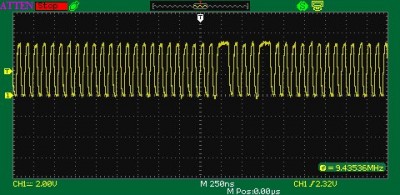
Starting with the clock stretching, both 1 and 2 wait states appear to be inserted as expected. Seen here with 1 wait state selected.
Attachment:
File comment: longer shot of the wait states
Wait states in action.jpg
Wait states in action.jpg [ 37.39 KiB | Viewed 993 times ]
The average frequency detected by the scope shows that particular section of code (probably keyboard scanning) has a 5 to 6% slowdown over all as the master clock is 20mhz for a nominal CPU speed of 10mhz. That's a small price to pay compared to running the board ad the speed of the slowest I/O component.

The first test runs were done with a slightly out of spec HC parts, both flip flops have been replaced with newly arrived AC parts and the clock from the flip flop shows a little ringing:
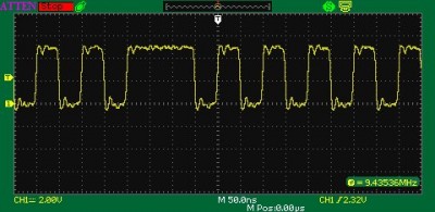
Attachment:
File comment: Scoping the clock side of the damping resistor
Before resistor.jpg
Before resistor.jpg [ 32.15 KiB | Viewed 993 times ]

On the CPU side of the 120R resistor the ringing is gone, but the waveform is somewhat rounded:
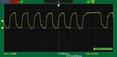
Attachment:
File comment: CPU side of the damping resistor
After resistor.jpg
After resistor.jpg [ 32.43 KiB | Viewed 993 times ]

Not that the CPU seems to mind, the rise and fall rate in the mid range is nice and fast.


Top
 Profile  
Reply with quote  
PostPosted: Thu Sep 16, 2021 4:03 pm 
Offline
User avatar

Joined: Thu May 28, 2009 9:46 pm
Posts: 8509
Location: Midwestern USA
Martin A wrote:
On the CPU side of the 120R resistor the ringing is gone, but the waveform is somewhat rounded...

Looks as though your clock circuit has higher-than-average parasitic capacitance, or your probe is loading down the circuit.

_________________
x86?  We ain't got no x86.  We don't NEED no stinking x86!


Top
 Profile  
Reply with quote  
PostPosted: Thu Sep 16, 2021 8:16 pm 
Offline

Joined: Sat Jan 02, 2016 10:22 am
Posts: 197
BigDumbDinosaur wrote:
Martin A wrote:
On the CPU side of the 120R resistor the ringing is gone, but the waveform is somewhat rounded...

Looks as though your clock circuit has higher-than-average parasitic capacitance, or your probe is loading down the circuit.

I wouldn't bet against either to be honest. The important thing is your design appears to be working as intended.


Top
 Profile  
Reply with quote  
PostPosted: Sat Sep 18, 2021 4:47 am 
Offline
User avatar

Joined: Thu May 28, 2009 9:46 pm
Posts: 8509
Location: Midwestern USA
J64C wrote:
Gotta post pics of the boards anyway though! Can’t leave us hanging. 8)

Here's a pic of the bad board and the good board. The bottom board is the good one.

Attachment:
pocV2.0_pcb_top02.jpg
pocV2.0_pcb_top02.jpg [ 3.42 MiB | Viewed 918 times ]

_________________
x86?  We ain't got no x86.  We don't NEED no stinking x86!


Top
 Profile  
Reply with quote  
PostPosted: Sat Sep 18, 2021 4:51 am 
Offline
User avatar

Joined: Thu May 28, 2009 9:46 pm
Posts: 8509
Location: Midwestern USA
BigDumbDinosaur wrote:
Quote:
The PCBs arrived on Monday, and as I was preparing to get the SMT stuff soldered in place, I discovered a major boo-boo in the layout...Supposedly, I'll have the new PCBs and stencil on Thursday.

The new boards and stencil arrived. The bus transceiver footprint is now correct. Time to build the contraption and see if she goes or blows.

Here are a few more pics.

Attachment:
File comment: POC V2.0 PCB Top Layer
pocV2.0_pcb_top.jpg
pocV2.0_pcb_top.jpg [ 2.09 MiB | Viewed 918 times ]
Attachment:
File comment: POC V2.0 PCB Bottom Layer
pocV2.0_pcb_bot.jpg
pocV2.0_pcb_bot.jpg [ 1.63 MiB | Viewed 918 times ]
Attachment:
File comment: POC V2.0 PCB w/SMT Components
pocV2.0_pcb_smt.jpg
pocV2.0_pcb_smt.jpg [ 1.92 MiB | Viewed 918 times ]

_________________
x86?  We ain't got no x86.  We don't NEED no stinking x86!


Top
 Profile  
Reply with quote  
Display posts from previous:  Sort by  
Post new topic Reply to topic  [ 86 posts ]  Go to page Previous  1, 2, 3, 4, 5, 6  Next

All times are UTC


Who is online

Users browsing this forum: No registered users and 34 guests


You cannot post new topics in this forum
You cannot reply to topics in this forum
You cannot edit your posts in this forum
You cannot delete your posts in this forum
You cannot post attachments in this forum

Search for:
Jump to: