6502.org Forum  Projects  Code  Documents  Tools  Forum
It is currently Sat Nov 23, 2024 1:16 am

All times are UTC


Post new topic Reply to topic  [ 298 posts ]  Go to page Previous  1 ... 3, 4, 5, 6, 7, 8, 9 ... 20  Next
Author Message
PostPosted: Thu Jan 30, 2020 1:06 am 
Offline
User avatar

Joined: Thu May 28, 2009 9:46 pm
Posts: 8507
Location: Midwestern USA
Proxy wrote:
also what about the idea of having both GND and Vcc in the Grid? like i showed in the picture? is it a good idea or somehow bad?

It may seem counter-intuitive, but the quality of ground connections in high-speed digital work is more important than the Vcc connections. This is due to a phenomenon we refer to as "ground bounce," which can cause circuit instability or outright failure.

Briefly explained, any given device relates its inputs to ground. For example, the minimum for a CMOS logic 1 is generally 70 percent of Vcc, measured relative to the internal ground in the device. If the device's connection to power supply ground is such that significant inductance or DC resistance (the combination of which is conventionally referred to as impedance) is introduced into the ground path, the effective value of the input will be less than it should be, due to the supposed ground in the device now being a fraction of a volt above true ground. If this effect is sufficient in magnitude, the device will effectively see something less than the 70 percent expected as logic 1, which could lead to undefined behavior.

A key to understanding how ground bounce can occur is understanding that the switching rates for CMOS logic are extremely rapid, often in the single-digit nanosecond range. Switching rates are largely independent of the system's clock rate, which is why a unit running with a sedate clock can still be plagued with ringing and ground bounce. Although CMOS logic uses very little current when quiescent, there will be a pronounced current spike as the device's output changes state. This spike will be a very short duration pulse, which effectively makes it a very high frequency pulse. Ergo your physical layout has to keep ground impedance to a minimum. Otherwise, that brief but intense spike will momentarily cause ground at the device to no longer be at ground potential—ground bounce.

The ideal construction would use a four-layer board with internal power and ground planes. There are several benefits, both physical and electrical in nature, to using a four-layer board. Routing becomes easier and component density can be greater, since board real estate doesn't have to be used to route power and ground. However, the biggest benefit is the almost-total elimination of ground bounce, and almost-total elimination of crosstalk between coincident traces on opposite sides of the board. Another benefit is the two inner layers look like a big bypass capacitor to the circuit, which does a lot to suppress switching noise.

If you opt for a two-layer board, which is fine for a lot of moderate speed digital work, concentrate on ground routing so return paths to power supply ground are as short and direct as possible. Each device should be bypassed to keep its current spikes from getting out onto Vcc and affecting other devices. Bypass capacitors should be placed as close to the device as possible, with the connection to the device's Vcc pin as short and direct as can be made. I use 0.1 µF, 50 volt, X7R MLCCs for bypassing purposes and also place low ESR electrolytics in various places to further dampen the effects of current gyrations. In the interest of minimizing the bypass capacitors' lead length and thereby reducing inductance, I use capacitors with 100 mil lead spacing.

As a fairly general rule in PCB layout, you should run north-south traces on one side of the board and east-west traces on the other side. The placement of angular traces will depend on where they are going. I usually place traces that mostly run northeast to southwest on the top of the board and northwest-southeast traces on the bottom. It's a judgment call that comes from experience.

I attached one of my board designs to give you some ideas. The red traces are on top, green on the bottom. This board is four-layer, and you can see where components are connected to the internal power and ground layers. This is one of my older layouts from when I was still using bypass capacitors with 300 mil lead spacing. Despite that, the computer I built on this board is stable at 14 MHz.

Attachment:
File comment: POC V1.1 PCB Layout
poc_v1.5.1_pcb.jpg
poc_v1.5.1_pcb.jpg [ 1.55 MiB | Viewed 2160 times ]

_________________
x86?  We ain't got no x86.  We don't NEED no stinking x86!


Top
 Profile  
Reply with quote  
PostPosted: Thu Jan 30, 2020 11:05 am 
Offline
User avatar

Joined: Fri Aug 03, 2018 8:52 am
Posts: 746
Location: Germany
So technically I should be completely fine if i just do grounding manually, then let some AutoRouter do the signals and Vcc lines? Or I just do both Ground and Vcc manually.

I still made a copy of my whole project because I want to try myself at the Grid design for grounding.
I'll do that later today though, I'm still on work and don't have KiCad here.


Top
 Profile  
Reply with quote  
PostPosted: Thu Jan 30, 2020 11:23 am 
Offline
User avatar

Joined: Thu Dec 11, 2008 1:28 pm
Posts: 10986
Location: England
(This article and video might be worth a look:
https://hackaday.com/2018/09/28/inducta ... the-fugly/
)

Note that Jeff's post upthread about a grid was illustrating only 4 squares: not nearly as fine as one square per chip.


Top
 Profile  
Reply with quote  
PostPosted: Thu Jan 30, 2020 3:35 pm 
Offline
User avatar

Joined: Fri Dec 11, 2009 3:50 pm
Posts: 3367
Location: Ontario, Canada
Proxy wrote:
what about the idea of having both GND and Vcc in the Grid? like i showed in the picture? is it a good idea or somehow bad?
No, it's not bad, but it takes more space, and one grid is almost as good; you don't really need two. That's assuming you have lots of bypass caps, which allow a ground grid to lend its stability to all the local Vcc points where the caps are located. (Or you could have a Vcc grid and let the caps lend its stability to all the local Gnd points where caps are located.)

There are a LOT of ways this can work, but here's one scheme that used to be quite common. Gnd and Vcc are on one side, with DIP's straddling them. And the Gnd lines tie together cross-wise on the opposite side.
Attachment:
BuMgtBz mod.png
BuMgtBz mod.png [ 41.37 KiB | Viewed 2122 times ]

BigEd wrote:
Note that Jeff's post upthread about a grid was illustrating only 4 squares: not nearly as fine as one square per chip.
It's true, the fineness of the grid can vary widely -- and there's no clear way to say how fine is "enough." But even having only 4 very coarse squares is a big improvement over some of the breadboard ground schemes I've seen! :roll:

-- Jeff

_________________
In 1988 my 65C02 got six new registers and 44 new full-speed instructions!
https://laughtonelectronics.com/Arcana/ ... mmary.html


Top
 Profile  
Reply with quote  
PostPosted: Thu Jan 30, 2020 4:25 pm 
Offline
User avatar

Joined: Fri Aug 03, 2018 8:52 am
Posts: 746
Location: Germany
another thing about the grid...
aren't you usually meant to avoid ground loops?
but a grid is literally made out of loops (since you're basically encasing ICs with ground traces). so how are loops bad but a bunch of them make a grid which is good?

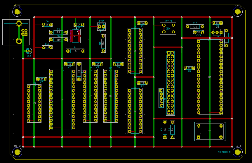
because this is what i currently designed and i'm not sure if i did it right.
Image

Image

maybe i misunderstood the definition of a grid, or people are just bad at naming stuff.
also i made sure pretty much all top traces are horizonal and all back traces are vertical.

and instead of 132x85mm it's now around 160x105mm


Top
 Profile  
Reply with quote  
PostPosted: Thu Jan 30, 2020 5:54 pm 
Offline
User avatar

Joined: Thu May 28, 2009 9:46 pm
Posts: 8507
Location: Midwestern USA
Proxy wrote:
another thing about the grid...
aren't you usually meant to avoid ground loops?
but a grid is literally made out of loops (since you're basically encasing ICs with ground traces). so how are loops bad but a bunch of them make a grid which is good?

because this is what i currently designed and i'm not sure if i did it right.
Image

Image

maybe i misunderstood the definition of a grid, or people are just bad at naming stuff.
also i made sure pretty much all top traces are horizonal and all back traces are vertical.

and instead of 132x85mm it's now around 160x105mm

I will be posting a more detailed response later on, but the short answer on ground loops is they tend to be more a problem with analogue circuits than digital ones. This is especially the case with vacuum tube amplifiers, in which the ground current flow varies widely depending on where in the circuit it is being measured.

_________________
x86?  We ain't got no x86.  We don't NEED no stinking x86!


Top
 Profile  
Reply with quote  
PostPosted: Thu Jan 30, 2020 9:07 pm 
Offline
User avatar

Joined: Fri Aug 30, 2002 1:09 am
Posts: 8544
Location: Southern California
The term "ground loop" is often misapplied, and the phenomenon is widely misunderstood. Countless times, I've given phone support to technicians installing our equipment in aircraft, where they misunderstand how noise is getting into the system, and they didn't follow our installation instruction manual, and they thought "ground is ground is ground," and thought they'd do better if they add a short connection from every part that's supposedly ground, to the airframe, or fail to isolate it as directed, and the result, as BDD alluded, is that noise from the alternator, the gyros, strobes, etc. got into the audio equipment. The tech would think he had to add a noise filter to the power supply line; but that's not where the noise was getting in.

What we have in digital PCB design is somewhat different, except where you have for example analog-to-digital (A/D) and digital-to-analog (D/A) converters on the same board with digital or switching power supply circuits. (I put all three on extremely dense boards in our products, and do keep the noise out.)

For your digital-only circuit, the previous links will help understand what's going on. Otherwise:
Proxy wrote:
So technically I should be completely fine if i just do grounding manually, then let some AutoRouter do the signals and Vcc lines? Or I just do both Ground and Vcc manually.
Autorouters save a lot of time but they're not very smart. You could sic the autorouter on the job, and then when it's done, manually 'sew' in a web of power and ground connections, using whatever room is left. It's not important that the grid be square. If adding a lot of these traces makes it look like the messy web certain spiders make (picture), it's ok. Without a ground plane, you're not going to have any real transmission lines anyway (which again is not that important for a small hobbyist board); but one of the next things is to minimize the inductance of connections from one IC's ground pin(s) to another IC's ground pins, which doesn't make the board cost any more. Look at the signals' ground-return current path length from one IC to another. Does it have to go down to the end of a row, over, and up the next row? Can you 'sew' in a shorter path? (Don't feel like you have to make all traces be at 0, 45, and 90 degrees. If you can make the path shorter by putting traces at odd angles, go for it.) For someone who was having trouble getting a solderless breadboard working (which is the most troublesome way to make this kind of circuits), Jeff has posted a good diagram or two pointing out these horrendously long paths, and how to shorten them. Maybe he can find it for us, since the point applies even though you're not using a solderless breadboard.

At the end of the day though, your board is small enough that I don't anticipate any actual malfunction from poor grounding practice; so I don't want fear of it to hold you up unduly, even though it's always good to try to understand this stuff better for future projects that get bigger and more ambitious.


Edit:
BigEd wrote:
(This article and video might be worth a look:
https://hackaday.com/2018/09/28/inducta ... the-fugly/ )
That's really good! The only thing I would modify is that the 32ns rise time he gives for 10MHz is much too slow for 65xx work. It's probably fine for other processors that take four clock cycles for a single memory access, but not 6502.

_________________
http://WilsonMinesCo.com/ lots of 6502 resources
The "second front page" is http://wilsonminesco.com/links.html .
What's an additional VIA among friends, anyhow?


Top
 Profile  
Reply with quote  
PostPosted: Thu Jan 30, 2020 9:50 pm 
Offline
User avatar

Joined: Fri Dec 11, 2009 3:50 pm
Posts: 3367
Location: Ontario, Canada
GARTHWILSON wrote:
Does it have to go down to the end of a row, over, and up the next row? Can you 'sew' in a shorter path?

Here is a clear and simple example of exactly this sort of thing. Two other examples of return-path remediation are here and here.

_________________
In 1988 my 65C02 got six new registers and 44 new full-speed instructions!
https://laughtonelectronics.com/Arcana/ ... mmary.html


Top
 Profile  
Reply with quote  
PostPosted: Fri Jan 31, 2020 7:50 am 
Offline
User avatar

Joined: Thu Dec 11, 2008 1:28 pm
Posts: 10986
Location: England
GARTHWILSON wrote:
At the end of the day though, your board is small enough that I don't anticipate any actual malfunction from poor grounding practice; so I don't want fear of it to hold you up unduly, even though it's always good to try to understand this stuff better for future projects that get bigger and more ambitious.

This is the important point here! There is such a thing as over-engineering, and when you give a bunch of engineers a chance to show off all their most arcane knowledge and their most obscure debugging stories, it's entertaining and informative but it may not be addressing the problem at hand.


Top
 Profile  
Reply with quote  
PostPosted: Fri Jan 31, 2020 10:51 am 
Offline
User avatar

Joined: Fri Aug 03, 2018 8:52 am
Posts: 746
Location: Germany
ok i think i got it. and yes while for a first and small project like this it's probably a bit over the top, it's still good to learn a bout these things like GarthWilson said.

also yea i've let the FreeRouter do it's thing and now i'm somewhat looking through it seeing if there are things i can make shorter.
somtimes i find something, but it mostly seems alright. (atleast to my untrained eyes)

and hey, i'm starting to get used to Routing, even if it's just fixing small mistakes of the FreeRouter.

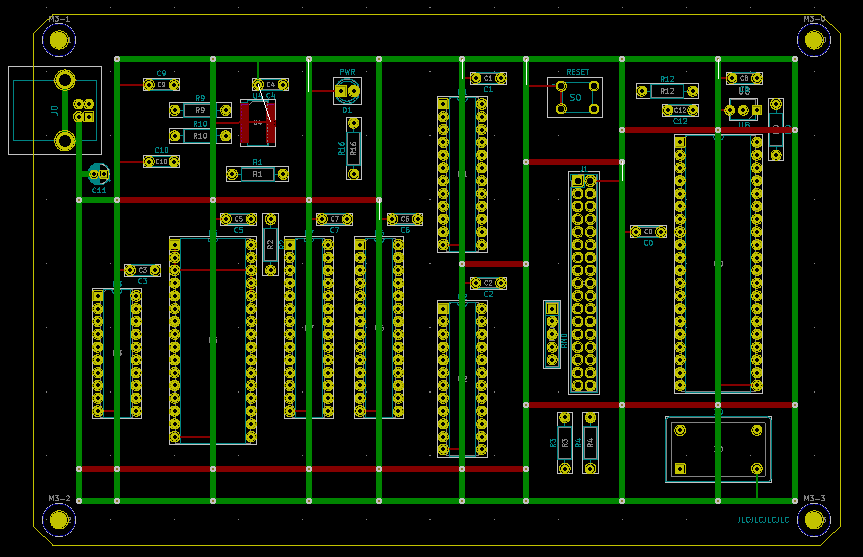
here is my new finished board design:

Both sides:
Attachment:
pcbnew_2020-01-31_11-47-03.png
pcbnew_2020-01-31_11-47-03.png [ 524.58 KiB | Viewed 2055 times ]

Top only:
Attachment:
2020-01-31_11-47-24.png
2020-01-31_11-47-24.png [ 357.31 KiB | Viewed 2055 times ]

Bottom only:
Attachment:
2020-01-31_11-47-17.png
2020-01-31_11-47-17.png [ 498.7 KiB | Viewed 2055 times ]


Top
 Profile  
Reply with quote  
PostPosted: Sun Feb 02, 2020 4:06 am 
Offline
User avatar

Joined: Fri Aug 03, 2018 8:52 am
Posts: 746
Location: Germany
I'll just take the lack of reponse as a "yep looks good"

though i'm still somewhat scared i missed something before ordering the PCBs.... but i don't know why.
it was already said that a ground grid for this is basically somewhat overkill, so i should especially not have any problems when i have one.


Top
 Profile  
Reply with quote  
PostPosted: Sun Feb 02, 2020 6:55 am 
Offline
User avatar

Joined: Fri Dec 11, 2009 3:50 pm
Posts: 3367
Location: Ontario, Canada
Proxy wrote:
it was already said that a ground grid for this is basically somewhat overkill, so i should especially not have any problems when i have one.
Right -- the grid looks good. But I will mention one little tweak you missed.

There will always be one more tweak -- it's endless! -- so I don't wanna be obsessive. :wink: But I think this is one that Garth was hinting at. So, for what it's worth, here it is.
Attachment:
Gnd grid.png
Gnd grid.png [ 30.53 KiB | Viewed 1998 times ]
GARTHWILSON wrote:
"Look at the signals' ground-return current path length from one IC to another. Does it have to go down to the end of a row, over, and up the next row? Can you 'sew' in a shorter path? (Don't feel like you have to make all traces be at 0, 45, and 90 degrees. If you can make the path shorter by putting traces at odd angles, go for it.)"

_________________
In 1988 my 65C02 got six new registers and 44 new full-speed instructions!
https://laughtonelectronics.com/Arcana/ ... mmary.html


Top
 Profile  
Reply with quote  
PostPosted: Sun Feb 02, 2020 1:39 pm 
Offline
User avatar

Joined: Fri Aug 03, 2018 8:52 am
Posts: 746
Location: Germany
ok i added that Ground Trace, and had to look through it again shorting some traces that the AutoRouter made longer than necessary.

it should now finally be ready to be ordered.

meaning i should also be able to order the parts from Mouser.


Top
 Profile  
Reply with quote  
PostPosted: Sun Feb 02, 2020 7:03 pm 
Offline
User avatar

Joined: Fri Aug 03, 2018 8:52 am
Posts: 746
Location: Germany
Here's what the hopefully finished thing looks like: (i know there are some minor oddities here and there but none of them should matter, plus i can't fix everything, especially not missing 3D Models)
Attachment:
2020-02-02_19-59-31.png
2020-02-02_19-59-31.png [ 423.94 KiB | Viewed 1969 times ]

Even added some Text to say what it is and show the Memory map (which i checked before adding... twice)

Vcc Traces are 0.55mm thick.
the GND Traces (from Grid to component) are 0.55mm thick.
the GND Grid Traces are 1.25mm thick.
the Signal Traces are 0.25mm thick.

only exception to this is the SMD Chip, where Vcc and GND are 0.3mm thick.

In Theory i should now be able to order it, and have no problems getting it to run. but i'm still nervous about actually buying it.
though they added another shipping option which is only 1/3 the price of DHL (6 EUR instead of ~20 EUR) but obviously takes a bit longer.
I think i'll go for that, i'd rather wait a few days longer than to spend too much money on a first board


Top
 Profile  
Reply with quote  
PostPosted: Thu Feb 06, 2020 4:25 pm 
Offline
User avatar

Joined: Fri Aug 03, 2018 8:52 am
Posts: 746
Location: Germany
Ok the Mouser parts have arrived, now i just need to wait on JLCPCB to finish the PCB and send it.


Top
 Profile  
Reply with quote  
Display posts from previous:  Sort by  
Post new topic Reply to topic  [ 298 posts ]  Go to page Previous  1 ... 3, 4, 5, 6, 7, 8, 9 ... 20  Next

All times are UTC


Who is online

Users browsing this forum: No registered users and 20 guests


You cannot post new topics in this forum
You cannot reply to topics in this forum
You cannot edit your posts in this forum
You cannot delete your posts in this forum
You cannot post attachments in this forum

Search for:
Jump to: