
Proxy wrote:
also what about the idea of having both GND and Vcc in the Grid? like i showed in the picture? is it a good idea or somehow bad?
Briefly explained, any given device relates its inputs to ground. For example, the minimum for a CMOS logic 1 is generally 70 percent of Vcc, measured relative to the internal ground in the device. If the device's connection to power supply ground is such that significant inductance or DC resistance (the combination of which is conventionally referred to as impedance) is introduced into the ground path, the effective value of the input will be less than it should be, due to the supposed ground in the device now being a fraction of a volt above true ground. If this effect is sufficient in magnitude, the device will effectively see something less than the 70 percent expected as logic 1, which could lead to undefined behavior.
A key to understanding how ground bounce can occur is understanding that the switching rates for CMOS logic are extremely rapid, often in the single-digit nanosecond range. Switching rates are largely independent of the system's clock rate, which is why a unit running with a sedate clock can still be plagued with ringing and ground bounce. Although CMOS logic uses very little current when quiescent, there will be a pronounced current spike as the device's output changes state. This spike will be a very short duration pulse, which effectively makes it a very high frequency pulse. Ergo your physical layout has to keep ground impedance to a minimum. Otherwise, that brief but intense spike will momentarily cause ground at the device to no longer be at ground potential—ground bounce.
The ideal construction would use a four-layer board with internal power and ground planes. There are several benefits, both physical and electrical in nature, to using a four-layer board. Routing becomes easier and component density can be greater, since board real estate doesn't have to be used to route power and ground. However, the biggest benefit is the almost-total elimination of ground bounce, and almost-total elimination of crosstalk between coincident traces on opposite sides of the board. Another benefit is the two inner layers look like a big bypass capacitor to the circuit, which does a lot to suppress switching noise.
If you opt for a two-layer board, which is fine for a lot of moderate speed digital work, concentrate on ground routing so return paths to power supply ground are as short and direct as possible. Each device should be bypassed to keep its current spikes from getting out onto Vcc and affecting other devices. Bypass capacitors should be placed as close to the device as possible, with the connection to the device's Vcc pin as short and direct as can be made. I use 0.1 µF, 50 volt, X7R MLCCs for bypassing purposes and also place low ESR electrolytics in various places to further dampen the effects of current gyrations. In the interest of minimizing the bypass capacitors' lead length and thereby reducing inductance, I use capacitors with 100 mil lead spacing.
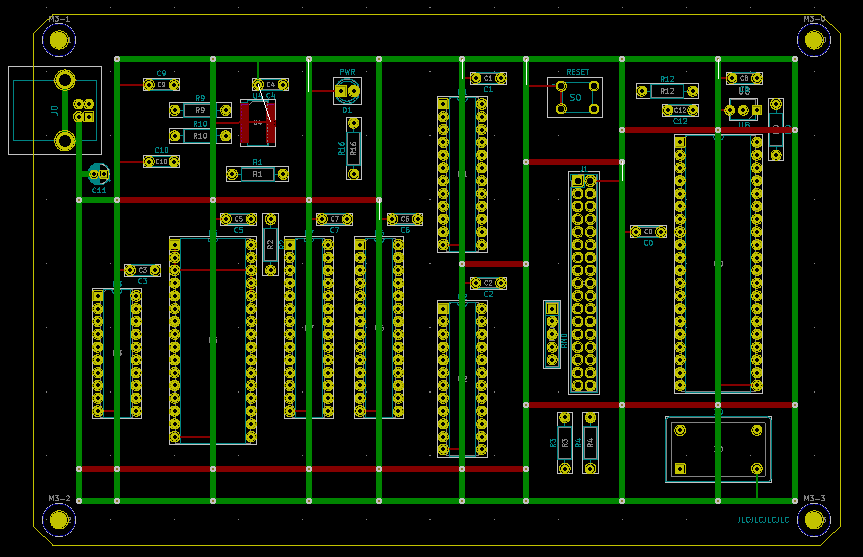
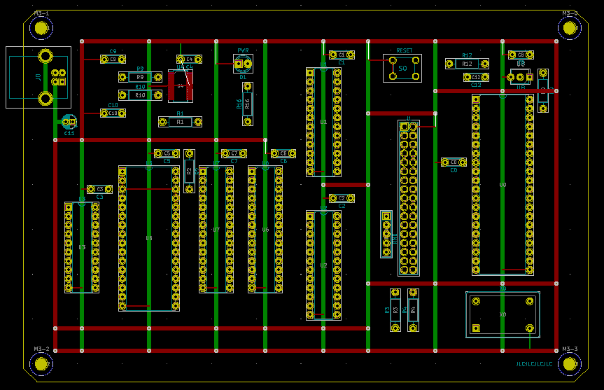
As a fairly general rule in PCB layout, you should run north-south traces on one side of the board and east-west traces on the other side. The placement of angular traces will depend on where they are going. I usually place traces that mostly run northeast to southwest on the top of the board and northwest-southeast traces on the bottom. It's a judgment call that comes from experience.
I attached one of my board designs to give you some ideas. The red traces are on top, green on the bottom. This board is four-layer, and you can see where components are connected to the internal power and ground layers. This is one of my older layouts from when I was still using bypass capacitors with 300 mil lead spacing. Despite that, the computer I built on this board is stable at 14 MHz.
- POC V1.1 PCB Layout


