6502.org Forum  Projects  Code  Documents  Tools  Forum
It is currently Thu Nov 21, 2024 1:02 pm

All times are UTC


Post new topic Reply to topic  [ 35 posts ]  Go to page 1, 2, 3  Next
Author Message
 Post subject: OT: stacked (DIP) chips
PostPosted: Mon May 30, 2016 9:07 pm 
Offline
User avatar

Joined: Thu Dec 11, 2008 1:28 pm
Posts: 10985
Location: England
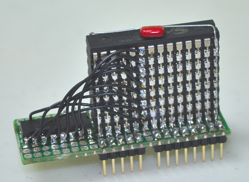
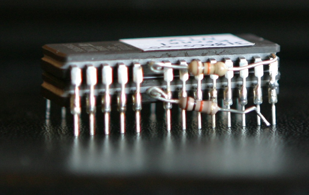
I thought this should be of interest: I collected some links to designs using stacked chips - mostly DIP chips - to get high density or to expand an existing circuit board with minimal work.

Richard Goedeken wanted to switch kernal ROMs in his Plus 4
http://www.fascinationsoftware.com/FS/h ... witch.html
Image

Duane Elscott made 4 towers of 16 SRAMs for a wirewrapped graphics board. From
http://web.archive.org/web/200406112215 ... tt/mem.htm
"If you're wondering why one of the stacks in the picture is taller than the rest, those were a different brand of ICs, with a slightly thicker body."
Image

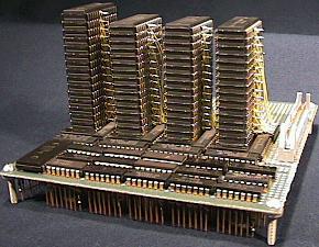
Timo Noko stacked 35 DRAMs to provide tagged lisp node storage in an Osborne luggable.
http://anycpu.org/forum/viewtopic.php?t=235&p=1456
Image

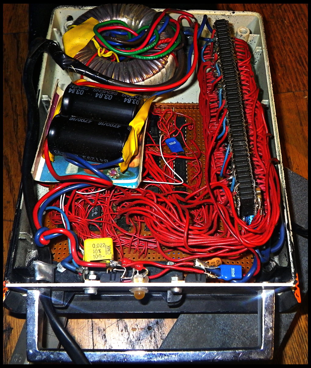
Garth Wilson stacks four 512Kx8 SRAMs on a DIP header to get 2Mx8, with a 74AC139 stood on edge at the end to select the right chip.
viewtopic.php?p=7564#p7564
Image

Garth Wilson's stack of 8 chips with a side order of decoder
viewtopic.php?f=4&t=2322&start=30
Image

(More from Garth on this page)

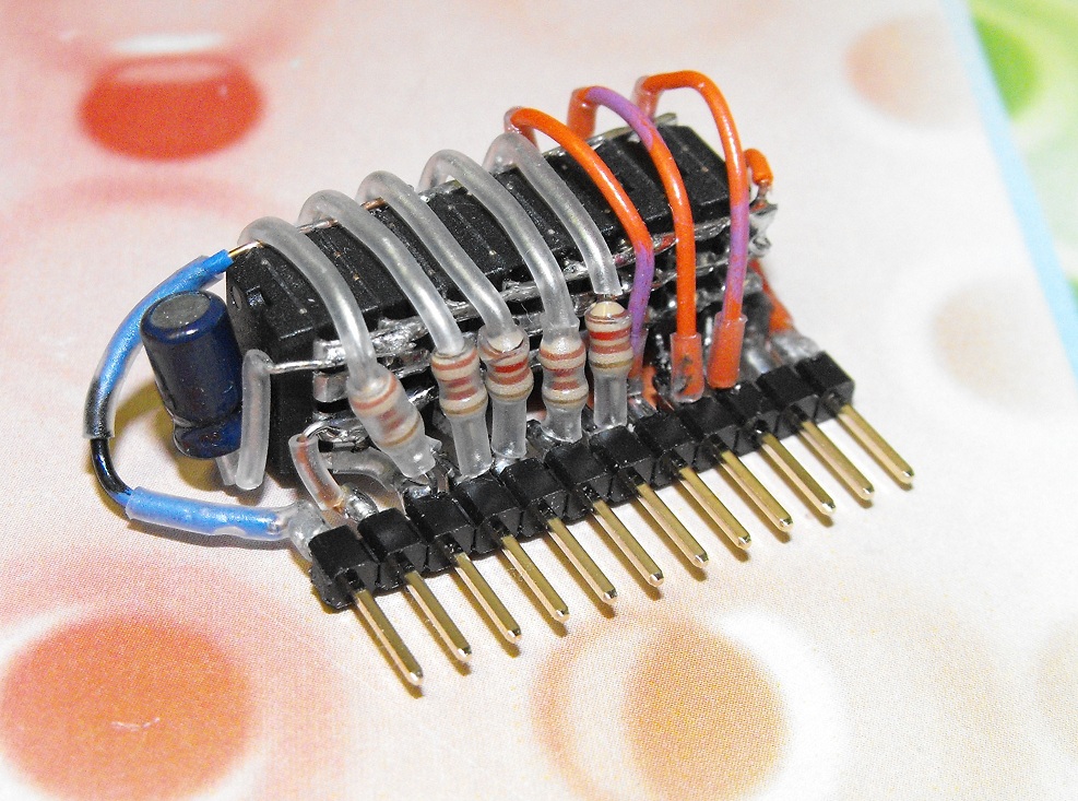
Duane Degn stacks 8 serial chips to make a byte serial memory
http://forums.parallax.com/discussion/1 ... it-version
Image

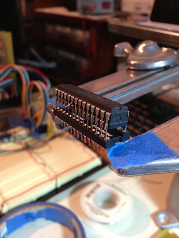
Quinn Dunki's Veronica machine piggybacks two RAMs
http://quinndunki.com/blondihacks/?p=1322
Image

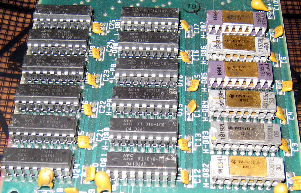
IBM's own 64k memory expansion for the 5150 PC used stacked chips.
http://www.minuszerodegrees.net/5150/ea ... _early.htm
Image

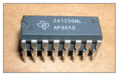
And again: this pair of 64Kbit, plastic-packaged DRAMs in DIPs have been stacked and soldered together at the Texas Instruments factory to produce a 128Kbit device with a small footprint. This product is destined for a socket in an IBM PC/AT clone that had broken the 640K barrier"
https://eda360insider.wordpress.com/201 ... packaging/
Image

Stacked chips in John Draper’s 24k Apple II, from "Captain Crunch’s Memory Modification" at
http://www.willegal.net/blog/?p=7246
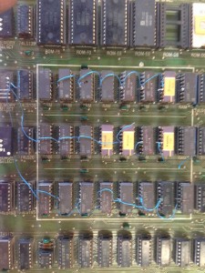
Image

Ronald Dekker stacks EPROM and SRAM in his "tiny but powerful stand alone BASIC microcomputer, not larger than the size of a package of cigarettes built entirely from salvaged components, just for fun!"
See
http://www.dos4ever.com/8031board/8031board.html
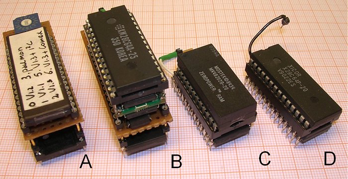
Image

"This early 1980s “advanced” calculator board included dual in-line packages (DIPs) stacked on top of each other."
http://electronicdesign.com/embedded/pa ... rospective
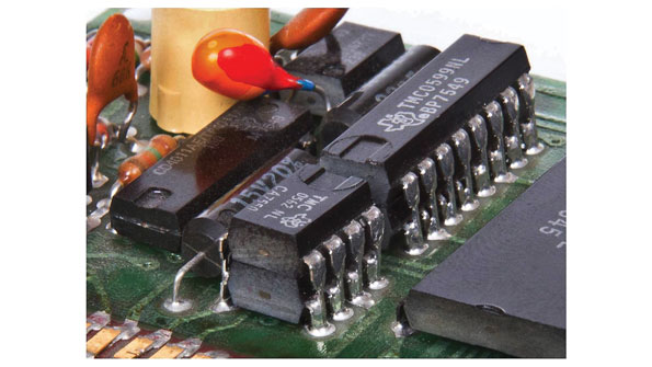
Image

Dave Curran discovered this stacked rom version switcher when refurbishing a ZX80
http://blog.tynemouthsoftware.co.uk/201 ... epair.html
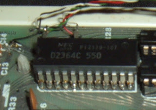
Image

[Previously posted on G+]


Last edited by BigEd on Mon May 18, 2020 5:54 am, edited 2 times in total.

Top
 Profile  
Reply with quote  
PostPosted: Tue May 31, 2016 1:12 am 
Offline
User avatar

Joined: Fri Dec 11, 2009 3:50 pm
Posts: 3367
Location: Ontario, Canada
Wow! -- some great work there. The byte serial memory is especially clever. And the 35-bit DRAM... :shock: Well!

I myself have often stacked chips, usually in unremarkable (though highly expedient) ways. But the photos below show a slight departure from the norm.

What we see is a Z80 SBC that features an 'hc574 used as an 8-bit output port. But because it was sometimes necessary to update fewer than all 8 bits there was a need to know what the existing data was. At first I managed that by maintaining a duplicate copy of the port's contents in RAM -- a workable but slightly cumbersome solution. It'd be better if the port itself could be read back... :idea:

Readback capability took the form of an 'hc245 soldered on top of the '574. As you can see, it was necessary to stagger the pins to make the appropriate connections line up!

-- Jeff
Attachment:
pins 1 to 10.jpg
pins 1 to 10.jpg [ 56.28 KiB | Viewed 16245 times ]
Attachment:
pins 11 to 20.jpg
pins 11 to 20.jpg [ 52.18 KiB | Viewed 16245 times ]

_________________
In 1988 my 65C02 got six new registers and 44 new full-speed instructions!
https://laughtonelectronics.com/Arcana/ ... mmary.html


Last edited by Dr Jefyll on Tue May 31, 2016 1:29 am, edited 1 time in total.

Top
 Profile  
Reply with quote  
PostPosted: Tue May 31, 2016 1:26 am 
Offline
User avatar

Joined: Thu May 28, 2009 9:46 pm
Posts: 8503
Location: Midwestern USA
Dr Jefyll wrote:
Readback capability took the form of an 'hc245 soldered on top of the '574. As you can see, it was necessary to stagger the pins to make the appropriate connections line up!

Yuh got all the angles covered. :D

_________________
x86?  We ain't got no x86.  We don't NEED no stinking x86!


Top
 Profile  
Reply with quote  
PostPosted: Tue May 31, 2016 1:27 am 
Offline
User avatar

Joined: Thu May 28, 2009 9:46 pm
Posts: 8503
Location: Midwestern USA
BigEd wrote:
I thought this should be of interest: I collected some links to designs using stacked chips - mostly DIP chips - to get high density or to expand an existing circuit board with minimal work.

Duane Elscott made 4 towers of 16 SRAMs for a wirewrapped graphics board. From
http://www.infinetivity.com/~delscott/mem.htm
"If you're wondering why one of the stacks in the picture is taller than the rest, those were a different brand of ICs, with a slightly thicker body."
Image

Reminds me of a public housing project for some reason.

_________________
x86?  We ain't got no x86.  We don't NEED no stinking x86!


Top
 Profile  
Reply with quote  
PostPosted: Tue May 31, 2016 8:42 pm 
Offline

Joined: Sat Dec 13, 2003 3:37 pm
Posts: 1004
BigEd wrote:
Timo Noko stacked 35 DRAMs to provide tagged lisp node storage in an Osborne luggable.
http://anycpu.org/forum/viewtopic.php?t=235&p=1456
Image


Nice. Seems like he embedded his own linear accelerator in there as well. Maybe he salvaged it from one of the Ghostbusters back packs.

Those photos are eerily creepy. Like photos of insects.


Top
 Profile  
Reply with quote  
PostPosted: Wed Jun 01, 2016 12:19 am 
Offline
User avatar

Joined: Mon May 25, 2015 2:25 pm
Posts: 690
Location: Gillies, Ontario, Canada
Those are some fine examples of RAM Stacks indeed!

Here is my 256K Stack, made with 15ns 32K SRAMs and a 3-8 decoder.
Great for dropping on a breadboard when you are out of 512K DIPs....

Image

Brad


Top
 Profile  
Reply with quote  
PostPosted: Tue Sep 04, 2018 3:08 pm 
Offline
User avatar

Joined: Thu Dec 11, 2008 1:28 pm
Posts: 10985
Location: England
These are neither stacked nor DIP, but I thought it fit in here. This is the 8-way stacked QIP-bearing "module" found in a 1985 Cray-2: 300 modules, 750 chips on each, several hundred watts from each module, immersed in 200 gallons of pumped inert coolant. AFAICT, most of the memory chips (75000 of them) would be 256kbit. The logic chips are 16-gate programmable. Four heavy duty CPUs running at 240MHz. More detail here.

Image


Last edited by BigEd on Fri Mar 29, 2019 5:45 pm, edited 1 time in total.

Top
 Profile  
Reply with quote  
PostPosted: Tue Sep 04, 2018 4:24 pm 
Offline

Joined: Sat Dec 13, 2003 3:37 pm
Posts: 1004
I'm going to have to say that I'm happy that I don't have to carry around 200 gallons of inert coolant to keep my iPhone from melting in to my leg every time I get a text.


Top
 Profile  
Reply with quote  
PostPosted: Tue Sep 04, 2018 5:18 pm 
Offline
User avatar

Joined: Wed Aug 17, 2005 12:07 am
Posts: 1250
Location: Soddy-Daisy, TN USA
What would be awesome is if someone made a complete SBC (without the board) using nothing but stacked IC's.

And no micro-contollers or PLD's. :-)

_________________
Cat; the other white meat.


Top
 Profile  
Reply with quote  
PostPosted: Tue Sep 04, 2018 6:09 pm 
Offline
User avatar

Joined: Tue Oct 25, 2016 8:56 pm
Posts: 362
Well, the problem you'd have there is the different package sizes and pin layouts. Stacked RAMs are relatively easy since only one pin needs to be seperately routed, but stacking a RAM, ROM, I/O, 6502 and Glue Logic would be a Frankenstein's Monster, methinks, not to mention a PITA to build.

_________________
Want to design a PCB for your project? I strongly recommend KiCad. Its free, its multiplatform, and its easy to learn!
Also, I maintain KiCad libraries of Retro Computing and Arduino components you might find useful.


Top
 Profile  
Reply with quote  
PostPosted: Tue Sep 04, 2018 6:34 pm 
Offline
User avatar

Joined: Wed Aug 17, 2005 12:07 am
Posts: 1250
Location: Soddy-Daisy, TN USA
Alarm Siren wrote:
Well, the problem you'd have there is the different package sizes and pin layouts. Stacked RAMs are relatively easy since only one pin needs to be seperately routed, but stacking a RAM, ROM, I/O, 6502 and Glue Logic would be a Frankenstein's Monster, methinks, not to mention a PITA to build.


Exactly. Which is why it would be awesome. ;-)

_________________
Cat; the other white meat.


Top
 Profile  
Reply with quote  
PostPosted: Tue Sep 04, 2018 6:56 pm 
Offline
User avatar

Joined: Fri Aug 30, 2002 1:09 am
Posts: 8543
Location: Southern California
That's quite a collection!

I seem to remember a small board from decades ago where memory was stacked on top of a 65xx IC (whether µP or I/O I can't remember).

Brad, I think I remember your stack which is probably in your picture, but your link to it just gives an error 404 message.

Here's a stack of four 74AC14's I used for driving a voltage multiplier to supply several watts:
Attachment:
74AC14x4.jpg
74AC14x4.jpg [ 33.07 KiB | Viewed 15366 times ]


Here's a dual MAX153 A/D converter:
Attachment:
DoubleMAX153.jpg
DoubleMAX153.jpg [ 28.04 KiB | Viewed 15366 times ]

This was for a workbench computer, but I have not implemented it yet.  The MAX153 is an 8-bit half-flash converter that's pretty quick.  If you run a 6502 at only 1MHz, you can put it on the bus and read it like a memory location.  When you select it, the conversion begins, and data is ready before the end of the phase-2 cycle; IOW, there's no need to start a conversion and come back later when it's done.  You can do the whole thing in one cycle.  I have a singe MAX153 on my main workbench computer, although there I go through a VIA since the clock is too fast to put the A/D right on the bus.  [Edit, 7/16/22:  I was just shopping for more parts, and found that the MAX153 has gotten super expensive, like $24US!  The somewhat slower ADC0820 is one-quarter to one-third the price.  The MAX114 seems to be the same thing inside as the MAX153 but is about half the price and yet has four input channels.  The MAX118 is the same thing for eight channels instead of four.  IOW, my two stacked converters above are now unnecessary.  I'm finding that all the fast A/D converters are expensive now though.  My purpose for the '153 is speed, and getting exact timing on the readings; so if you don't need the speed but you want more resolution, you you could use SPI or I²C A/D converters, perhaps putting them in SPI-10 or I2C-6 or 65SIB devices you plug into those ports on your computer.]

My stacked 512Kx8 SRAMs in Ed's pictures above were things that eventually led up to the 4Mx8 10ns 5V SRAM module I offer, with parts on both sides:
Attachment:
ModuleStraightPins.jpg
ModuleStraightPins.jpg [ 40.16 KiB | Viewed 15366 times ]

I have three different connector options.

Stacking made good use of space; but besides being kind of messy, it was too labor-intensive to do a lot of, like to supply modules to others for their projects.  Putting parts on both sides can be done with thru-hole parts too, if you stagger the rows of IC pins.  You can either use socket strips on the first side so the other side can be soldered before putting the IC in the first side, or you have to be able to solder the ICs from the top of the pins instead of under the board.
Attachment:
DIPbothSides1.jpg
DIPbothSides1.jpg [ 52.98 KiB | Viewed 15366 times ]

Attachment:
DIPbothSides2.jpg
DIPbothSides2.jpg [ 100.65 KiB | Viewed 15366 times ]

_________________
http://WilsonMinesCo.com/ lots of 6502 resources
The "second front page" is http://wilsonminesco.com/links.html .
What's an additional VIA among friends, anyhow?


Top
 Profile  
Reply with quote  
PostPosted: Tue Sep 04, 2018 7:06 pm 
Offline
User avatar

Joined: Wed Aug 17, 2005 12:07 am
Posts: 1250
Location: Soddy-Daisy, TN USA
As Dave would say, all of the electrons are going to fall out!

_________________
Cat; the other white meat.


Top
 Profile  
Reply with quote  
PostPosted: Tue Sep 04, 2018 7:10 pm 
Offline
User avatar

Joined: Tue Oct 25, 2016 8:56 pm
Posts: 362
cbmeeks wrote:
Alarm Siren wrote:
Well, the problem you'd have there is the different package sizes and pin layouts. Stacked RAMs are relatively easy since only one pin needs to be seperately routed, but stacking a RAM, ROM, I/O, 6502 and Glue Logic would be a Frankenstein's Monster, methinks, not to mention a PITA to build.


Exactly. Which is why it would be awesome. ;-)


Challenge Accepted.

_________________
Want to design a PCB for your project? I strongly recommend KiCad. Its free, its multiplatform, and its easy to learn!
Also, I maintain KiCad libraries of Retro Computing and Arduino components you might find useful.


Top
 Profile  
Reply with quote  
PostPosted: Tue Sep 04, 2018 7:50 pm 
Offline
User avatar

Joined: Wed Aug 17, 2005 12:07 am
Posts: 1250
Location: Soddy-Daisy, TN USA
Alarm Siren wrote:
Challenge Accepted.


Now, I would say PLCC-44 only for MPU and I/O but I think the Geneva Convention prohibits that kind of torcher.

:-D

_________________
Cat; the other white meat.


Top
 Profile  
Reply with quote  
Display posts from previous:  Sort by  
Post new topic Reply to topic  [ 35 posts ]  Go to page 1, 2, 3  Next

All times are UTC


Who is online

Users browsing this forum: No registered users and 7 guests


You cannot post new topics in this forum
You cannot reply to topics in this forum
You cannot edit your posts in this forum
You cannot delete your posts in this forum
You cannot post attachments in this forum

Search for:
Jump to: