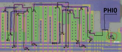
Complete 6502 interrupt processing circuit.
And short description.
Input pads /NMI, /IRQ, /RES are saved in input triggers.
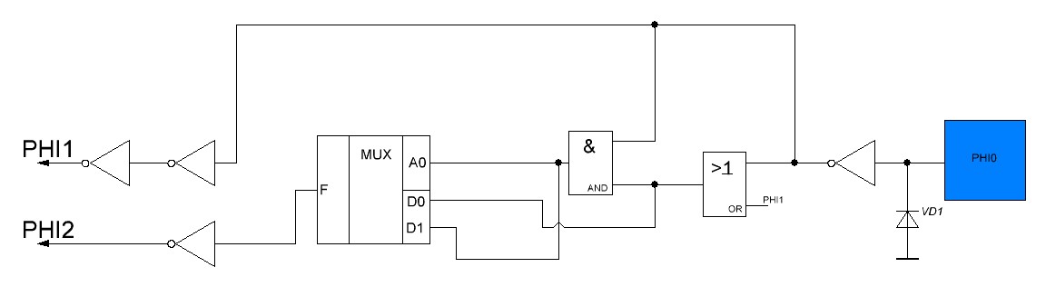
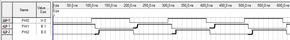
Interrupt generation circuit additionally requires 6 and 7 cycles (since they do not arrive from decoder) (control signals BRK6E and BRK7). Control signal BRK6E begins during the PHI2 of 6th cycle and ends during PHI1 of 7th cycle (overlap 6 and 7 cycle). This is done in order to determine the edge of the signal /NMI. Edge detection of /NMI based on classic edge detect circuit (two cross-coupled RS-triggers).
The signal /RES is further saved on the RESET FLIP/FLOP, as it is required for other random logic circuits (in particular for a special control of R/W pad during reset).
The fact of the arrival of any interrupt reflected on B-flag, the output of which (B_OUT) forces the processor to execute BRK instruction (opcode 0x00). Thus developers unified processing of all interrupts.
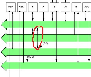
Last small circuit generates an interrupt address (or vector) (control lines 0/ADL0, 0/ADL1 and 0/ADL2), which is reflected on 3 bits of the address bus.
The interesting thing is affection of BR2 (Branch T2) and T0 (Execute Cycle 0) control lines on interrupt detection (IRQ CHECK).
In case you wish to play with it in
Logisim, you can grab it from SVN:
https://code.google.com/p/breaks/source ... 2/INT.circ
PS. All D-latches are level-triggered. Those one with invertor are PHI1 driven (and in turn PHI2 driven without it).