
Hi.
I'm going to write very low-level emulator of 6502, based on chip images made by Visual6502 team.
I will repost my digging here, from emu-russia board.
Source and explanations (on russian) : http://forum.emu-russia.net/viewtopic.php?f=13&t=3938
Progress:
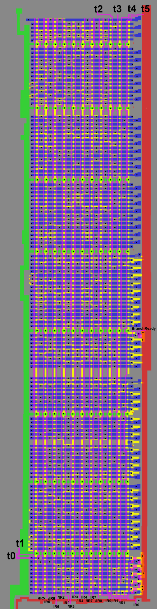
T-step shift register: Circuit Simulation
PLA: Circuit Simulation
Instruction Register: Circuit Simulation
Interrupt priority: Circuit
Predecode Logic: Circuit Simulation
Random Logic: Circuit
Registers: Circuit Simulation
ALU: Circuit Simulation (partial)
Program Counter: Circuit Simulation
Address Bus: Circuit Simulation
Data Latch: Circuit
Miscellaneous pads logic: Circuit Simulation
6502 Overview
Breaking 6502 apart
Breaking 6502 apart
Last edited by org on Mon Oct 15, 2012 11:18 am, edited 18 times in total.
6502 addict
Re: Breaking 6502 apart
Todays speccy : Timing control.
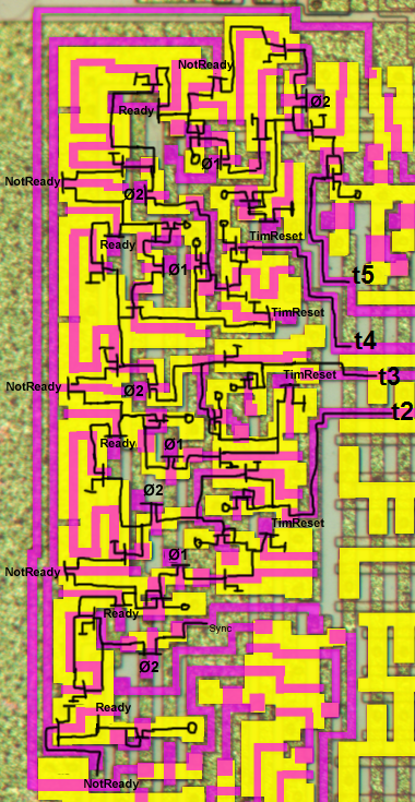
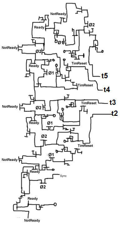
TimReset control goes from "random logic" and its purpose to set all T-outputs high.
Low level T-ouput fires PLA line.
TimReset control goes from "random logic" and its purpose to set all T-outputs high.
Low level T-ouput fires PLA line.
6502 addict

Re: Breaking 6502 apart
Hi Org
Welcome to the forum! You've done some impressive tracing and diagramming there. It's good to have a picture of how the transistors are laid out in 2D - a combination of the circuit design and the layout design.
If you want it, you can get the transistor-level circuit from the visual6502 website, with a little text processing. The enhancement-mode (pull-down and pass) transistors are defined in the file
http://visual6502.org/JSSim/transdefs.js
and the pull-up transistors are found as '+' annotations in
http://visual6502.org/JSSim/segdefs.js
Many of the numbered nodes have names defined in
http://visual6502.org/JSSim/nodenames.js
The transdefs file has some semi-useful information about the transistor location and sizes, but not the exact geometry.
Hope you find that useful, and hope to hear more from you as you make progress with your model!
Cheers
Ed
Re: Breaking 6502 apart
Can anyone, briefly, explain what we're looking at, at all? I understand it's a picture of an actual chip. Are each of this T-ish shape things transistors or are they logic gates? a zillion NAND gates?
I assume eventually these all terminate in to their respective pin of the original 40 pins on the chip?
Not my field, so I can't really make heads or tails of it -- just passive following along, nodding my head, and going "uh-huh".
I assume eventually these all terminate in to their respective pin of the original 40 pins on the chip?
Not my field, so I can't really make heads or tails of it -- just passive following along, nodding my head, and going "uh-huh".
Re: Breaking 6502 apart
This is part of internal chip schematics. And those pi-like things are individual transistors, drawn on top of chip layout )
6502 addict
Re: Breaking 6502 apart
org wrote:
Can someone explain why phi2 is integrated into flip-flop ? 
Cheers
Ed
Re: Breaking 6502 apart
whartung wrote:
...a zillion NAND gates?
Quote:
I assume eventually these all terminate in to their respective pin of the original 40 pins on the chip?
Simulating the circuit turns out to be a challenge because at least 16 of the transistors truly act bidirectionally. Information flows in both directions (one way, but different ways during different operations.) An actual circuit simulator has no difficulty, but has terrible performance. These 16 are the connections the Special Bus makes to the other busses in the datapath. (See Hanson's block diagram.)
Cheers
Ed
Re: Breaking 6502 apart
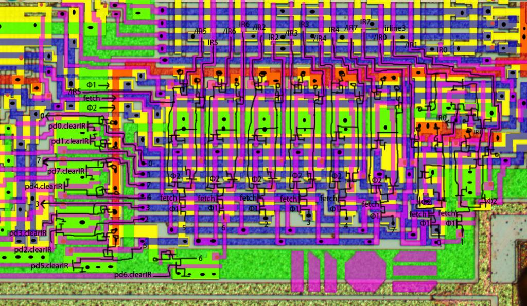
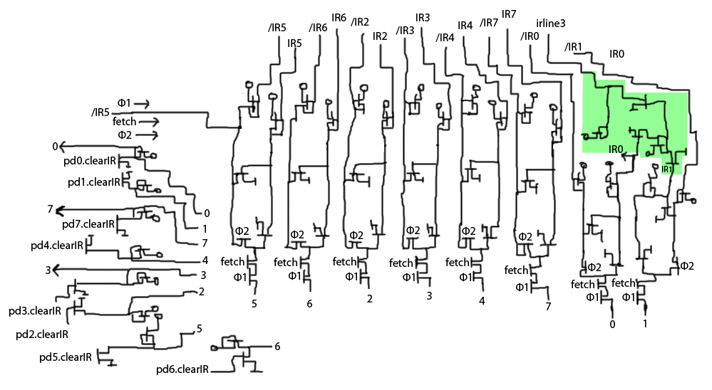
Todays speccy : instruction decoder (PLA)
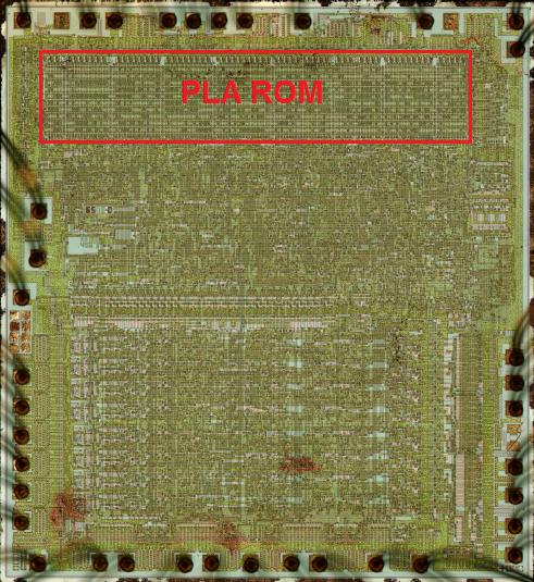
I will not draw transistor-level schematics, because its trivial.
I will not draw transistor-level schematics, because its trivial.
6502 addict

Re: Breaking 6502 apart
Todays speccy : Data bus + data latch
Complete picture:
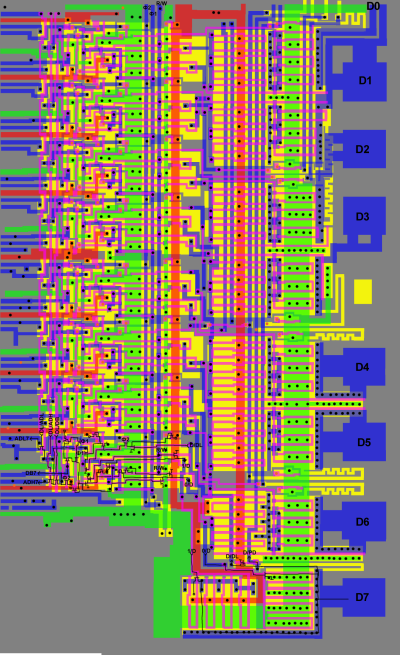
Data pin:
Data latch:
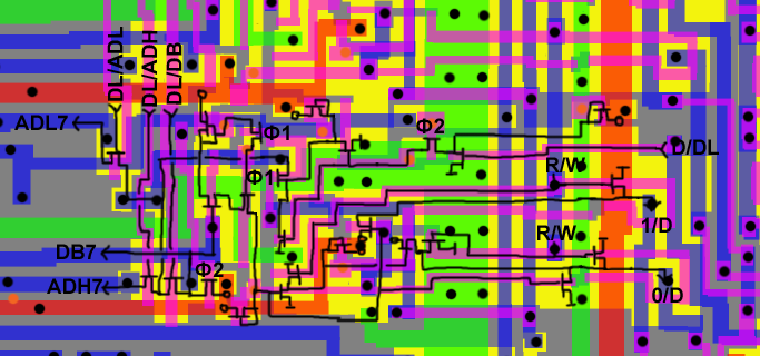 (not yet recognized where actually is "latch" )
Data latch and data pin are regular structures and multiple x8 )
Complete picture:
Data pin:
Data latch:
6502.org wrote:
Image no longer available: http://ogamespec.com/imgstore/whc4fec8adeeb2a5.jpg
Data latch and data pin are regular structures and multiple x8 )
6502 addict
Re: Breaking 6502 apart
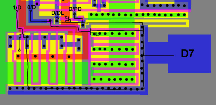
To find a (dynamic) latch, look for a transistor gate which is floating when a clock is low. In this case, from the D/DL annotation on the right, go left through the pulldown of the inverter, then left again through the Phi2 transistor, and you've arrived at the latch. You actually have two transistor gates but the two transistors are in parallel and have the same electrical function as each other - it's a single transistor.
The parasitic capacitance of a transistor gate is the largest type of stray capacitance on a chip of this type, and is used as the storage node of the latch.
Hope this helps
Cheers
Ed
The parasitic capacitance of a transistor gate is the largest type of stray capacitance on a chip of this type, and is used as the storage node of the latch.
Hope this helps
Cheers
Ed
Re: Breaking 6502 apart
Do you know, how long this sort of capacitor memory can hold the charge ?
Let say, CPU is in "read mode" (phi2 is high). Will data latch keep its charge during CPU "write mode" (when phi1 is high) ?
Let say, CPU is in "read mode" (phi2 is high). Will data latch keep its charge during CPU "write mode" (when phi1 is high) ?
6502 addict
Re: Breaking 6502 apart
That's related to the question of how slow a clock can you reliably run an NMOS 6502. I don't know the answer. But a DRAM of that era likes to be refreshed every 2ms, so I'd use that as an order of magnitude estimate: the capacitor structure is the same, although the sensing of charge is different. I think this is consistent with being able to run down to kHz but not slower.
Certainly there is no hard cutoff: the charge will leak, and the rate of leakage is a function of temperature and variations of each transistor. Eventually the voltage is too low for the pulldown to be effective: the logic gate's output rises high enough for the next gate to pull down.
Cheers
Ed
Edit: DRAM refresh period (but I'm still not sure if it was 2ms or 8ms)
Edit: This datasheet is for NMOS 6500 series and says 50kHz is the minimum clock frequency (top of page 5) - revision date 11/85.