65Org16.x Dev. Board V1.1 using a Spartan 6 XC6SLX9-3TQG144

Topics relating to PALs, CPLDs, FPGAs, and other PLDs used for the support or creation of 65-family processors, both hardware and HDL.
Post Reply
ElEctric_EyE
Posts: 3260
Joined: 02 Mar 2009
Location: OH, USA

65Org16.x Dev. Board V1.1 using a Spartan 6 XC6SLX9-3TQG144

Post by ElEctric_EyE »

Progress continues to put the 65Org16.b (16-bit NMOS6502 without decimal mode) into action. 65Org16.a is BigEd's original creation based on Arlet's Verilog NMOS6502 softcore. Arlet & BigEd both continue to refine their work on GitHub, as I do when I find time. I would like to add a 65Org16.c core soon, which would have some simple but excellent time saving opcodes, like PHX,PHY,PLX, and PLY. I'll revisit that thread when I get most of this other stuff sorted out...

Currently I'm working on I2C drivers. Also, when I hit a roadblock I'm trying to sift out 1 of 3 6502 Assemblers/Disassemblers (Micromon-64, SuperMon-64, and Hashmon) that will reside in the FPGA BRAM. Looking at the code of all 3, I'm trying to determine all the JMPs/JSRs outside of the code. Looking and comparing the binaries reconstituted through MK's assembler, together with the book 'Mapping the 64', I should be able to make a choice soon.

V1.0 was a failure because the SDRAM layout was incorrect. Took 2 months for that initial iteration. From that version I learned that the MCP2200 appears to function properly with the Br@y terminal working under Windows, when it is fed 10MHz. I say "appears" because I could only look at the transmit and receive LEDs. I really had no drivers for any output devices. This was another shortsighted design error of V1.0...

Enter V1.1:
It's taken an additional 2 months, but I've added a 800x480 TFT touchscreen display interface connector, an I2C touchscreen controller IC and connector, narrowed the traces to .006", added 3 I2C programmable oscillators for 3 IOB's and changed the CS4954 video interface to I2C from parallel. Also the 100MHz clock now goes to all 4 IOB's.
The display I've chosen is a step-up from a similar display I've used successfully with Xilinx FPGA's in my 6502SoC. I was limited to 38MHz in that design, and expect to be limited here as well because it uses the same 8-bit SSD1963 controller and uses Phase 2 as the clock source. This is good because I can recycle the software I've written for the display with some minor changes, but it's bad because the CPU core has the ability to run faster than 38MHz. However, the display is really only being used to make and test drivers. The top_level schematic design is very similar to one of the last posts on the 6502SoC.

Unlike the 6502SoC though, this V1.1 of the DevBoard is almost all HDL. 3 files are schematic based, 2 address decoding files and the Top_Level schematic. Ideally I would like to convert the 2 address decoding into verilog, like I converted my ORs module.

Here's the Memory Map:

Code: Select all

				      65Org16 V1.1 DEVELOPMENT BOARD MEMORY MAP

		      $0000_0000 - $0000_03FF....................HESMON/OS VARIABLES
		      $0000_0400 - $0000_07FF....................VIDEO MATRIX (40x25)
	8K	    $0000_0800 - $0000_1BFF....................EXTENDED VIDEO MATRIX (100X60)
		      $0000_1C00 - $0000_1FFF....................AVAILABLE ZERO PAGE AS FPGA BLOCK RAM

	56K	   $0000_1000 - $0000_FFFF....................UNUSED - REMAINDER 65Org16 ZERO PAGE

	60K	   $0001_0000 - $0001_EFFF....................UNUSED - REMAINDER 65Org16 STACK

	4K	    $0001_F000 - $0001_FFFF....................AVAILABLE STACK AS FPGA BLOCK RAM

	4.3GB	 $0002_0000 - $FFFE_FFFF....................UNUSED

		      $FFFF_0000 - $FFFF_0007....................I2C REGISTERS
		      $FFFF_0008 - $FFFF_0009....................PS2 REGISTERS
		      $FFFF_000A - $FFFF_000D....................SPI REGISTERS
	48K	   $FFFF_OOOE - $FFFF_000F....................UART REGISTERS
	I/O      $FFFF_0010 - $FFFF_0011....................TFT REGISTERS
		      $FFFF_0012.................................16-BIT PSEUDORANDOM NUMBER GENERATOR (READ ONLY)
            $FFFF_0013 - $FFFF_001F....................UNUSED DECODED
		      $FFFF_0020 - $FFFF_BFFF....................UNUSED

		      $FFFF_C000 - $FFFF_CFFF....................HESMON
		      $FFFF_D000 - $FFFF_DFFF....................OS,DRIVERS,CHARACTER PIXEL DATA
	16K	   $FFFF_E000 - $FFFF_FFF9....................AVAILABLE SYSTEM MEMORY AS FPGA BLOCK RAM
		      $FFFF_FFFA - $FFFF_FFFB....................NMI VECTOR
		      $FFFF_FFFC - $FFFF_FFFD....................RESET VECTOR
		      $FFFF_FFFE - $FFFF_FFFF....................IRQ/BRK VECTOR
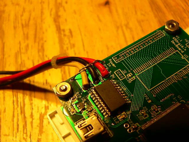
8:51 AM 1/7/2012
Here are some pics of the construction. No soldering errors this time!

Errors: Silkscreen is covering where I wanted to solder main power wires, but those wires have been secured the way I've envisioned!
Image
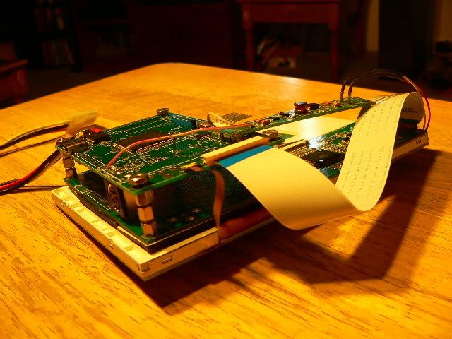
I've used 3M double sided tape on a V1.0 board and use it as a mount for the V1.1 (on top) with some vertical standoffs to position it to make room for the PS2 keyboard connector that is shown on the left, on the bottom. Also in the forefront, is the 4-pin .5mm FFC, for the touchscreen panel, and the 20-pin 1mm FFC cables and connectors, for the TFT display.
Image
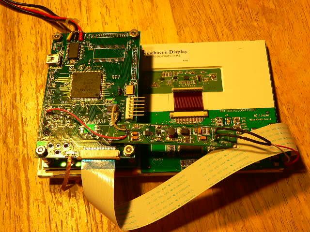
Here you can more clearly see the interconnections. The small board on the bottom right, with 2 wires going in on the left and 2 wires going out, is the DC-DC converter for the LED backlight driver for the TFT. I initially tried 3.3V in, but it was using large amounts of current as it was dragging the 3.3V supply down to 2.5V. Thankfully no damage was done to the board.
Image

This is my parts list to date. Most have been copied over from V1.0, so it is still not up to date for V1.1 as it is still under development. But all the IC's that have been planned for on the circuit board are listed...

Code: Select all

					65Org16.x V1.1 Development Board Parts List	(6/8/2011-12/2011...)

QTY	Price	    Description               Part#                       Package            	Supplier			   Sch. ID
 1	$6.95     FPGA Prom                 XCF04S	                    20-pin TSSOP   	    Digi-Key			   U2
 1	$18.63    FPGA                      XC6SLX9-3TQG144I            144-pin QFP   	    AvnetExpress		 U1
 1	$7.38     Video Controller 		      CS4954                      48-pin QFP      	  AvnetExpress		 U4
 1	$5.23	    16MBx16 SDRAM 167MHz      MT48LC16M16A2P-6A:D	        54-pin TSOPII     	AvnetExpress		 U3
 1	$1.24     8Mb SPI Flash             SST25VF080B-80-4I           8-pin SOIC     	    Digi-Key			   U10
 1	$0.81     3.3V POReset Supervisor   DS1818R-10+CT-ND            SOT-23	            Digi-Key			   U5
 1	$0.74     2.5V 1A VRegulator      	MCP1826S-2502E/DB-ND        SOT-223-3         	Digi-Key			   U7
 1	$0.74     1.2V 1A VRegulator     	  MCP1826S-1202E/DB-ND        SOT-223-3         	Digi-Key/Mouser	 U8
 1	$4.02	    100MHz 3.3VOsc. HCMOS/TTL	CTX318LVCT-ND		            SMD			            Digi-Key			   U6
 1	$2.12	    USB to UART			          MCP2200-I/SO-ND		          20-pin SOIC		      Digi-Key			   U9
 3	$6.75	    touch screen controller	  296-14340-1-ND		          16-pin TSSOP		    Digi-key
 3	$?	      3.3V 4kHZ-66MHz Prog Osc	DS1085LZ-5+T		            8-pin SOIC

 3	$0.76	    1ea 22uF 6.3V capacitor	  445-1595-1-ND		            1210			          Digi-Key		     C33,C34,C35
 2	$0.53	    1ea 4.7uF 10V capacitor	  587-1379-1-ND		            1210			          Digi-Key			   C31,C32
 5	$0.74	    10ea .1uF 6.3V capacitor	709-1009-1-ND		            0603			          Digi-Key		     C1-C30,C36-C42
 5	$0.06	    10ea .01uF 16V capacitor	490-1525-1-ND		            0603			          Digi-Key	       Alternate to .1uF
 1	$0.16	    10ea 470nF capacitor	    490-1548-1-ND		            0603			          Digi-Key			   C43
 6	$0.02	    1ea 0ohm resistor jumper	P0.0GCT-ND			            0603			          Digi-Key		     J1-J4,J10
 3	$0.02	    1ea 100ohm resistor		    P100GCT-ND			            0603			          Digi-Key		     R1-R5,R10,R11
 2	$0.02	    1ea 75ohm resistor		    P75GCT-ND			              0603			          Digi-Key			   R6,R7,R12
 2	$0.02     1ea 300ohm resistor		    P300GCT-ND			            0603			          Digi-Key			   R6,R7,R12
 2	$0.56	    1ea 5K trimpot		        3302W-502ECT-ND		          SMD			            Digi-Key			   R8,R9
 3	$0.02	    1ea 330 resistor		      P330GCT-ND			            0603			          Digi-Key	       R13,R15,R16,R17
 2	$0.02	    1ea 4.7Kohm resistor	    P4.7KGCT-ND			            0603			          Digi-Key		     J5,J6,R19,R20
 1	$0.02	    1ea 3.9Kohm resistor      P3.9KGCT-ND			            0603			          Digi-Key			   R14
 1	$0.02	    1ea 470ohm resistor		    P470GCT-ND			            0603			          Digi-Key			   R18
 1 	$0.56	    1ea blue LED			        160-1647-1-ND		            0603			          Digi-Key			   L1
 1	$0.52	    1ea green LED			        160-1435-1-ND		            0603			          Digi-Key			   L2

 1	$1.10	    RCA Jack Blue			        CP-1404-ND			            r. angle thru-hole	Digi-Key			   K6
 1	$1.41	    6-pos mini din PS/2		    CP-4060-ND			            r. angle thru-hole	Digi-Key			   K5
 1	$1.29	    4-pos mini din S-Video	  CP-2240-ND			            r. angle thru-hole  Digi-Key			   K3
 3	$2.99	    40-pin .050 male header   609-3724-ND			            H1-3 mating adapter	Digi-Key			   future
 3	$4.41	    40-pin .050 female recep  609-3766-ND			            thru-hole		        Digi-Key		     H1,H2,H3
 1	$0.69	    mom push switch white	    SW415-ND			              SMD			            Digi-Key			   S1	
 1	$0.69	    mom push switch yellow	  SW416-ND			              SMD			            Digi-Key			   S2
 1	$0.63	    6-pin .1 male SIP 		    A1918-ND			              r. angle thru-hole  Digi-Key			   K2
 
 1	$1.98	    1ea mini USB			        A31727CT-ND			            SMD 			          Digi-Key			   K8

 
 10	$0.20	    .050" jumper			        S9014E-03-ND		            thru-hole		        Digi-Key
 10	$0.24	    .050" jumper short		    S9345-ND						                            Digi-Key
 1	$0.86	    .5mm 4-pos FFC connector	OR746CT-ND					                            Digi-Key
 1	$2.34	    1mm 20-pos FFC connector	WM7964CT-ND					                            Digi-Key
 10	$0.02	    1.2Kohm resistor		      P1.2KGCT-ND					                            Digi-Key
 10	$0.05	    .1uF 10V			            399-1095-1-ND		            0603			          Digi-Key
 5	$0.02	    1ea 47Kohm resistor		    P47KGCT-ND			            0603			          Digi-Key
Here is the V1.1 DevBoard Layout:
Image

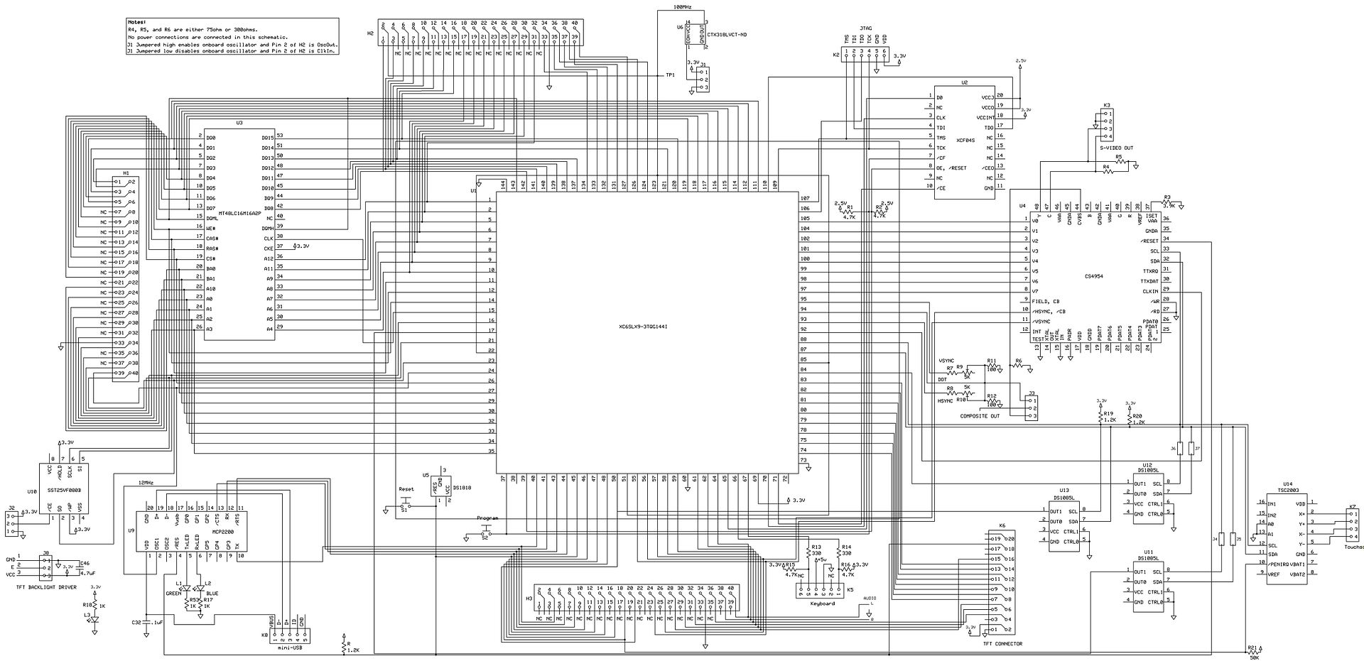
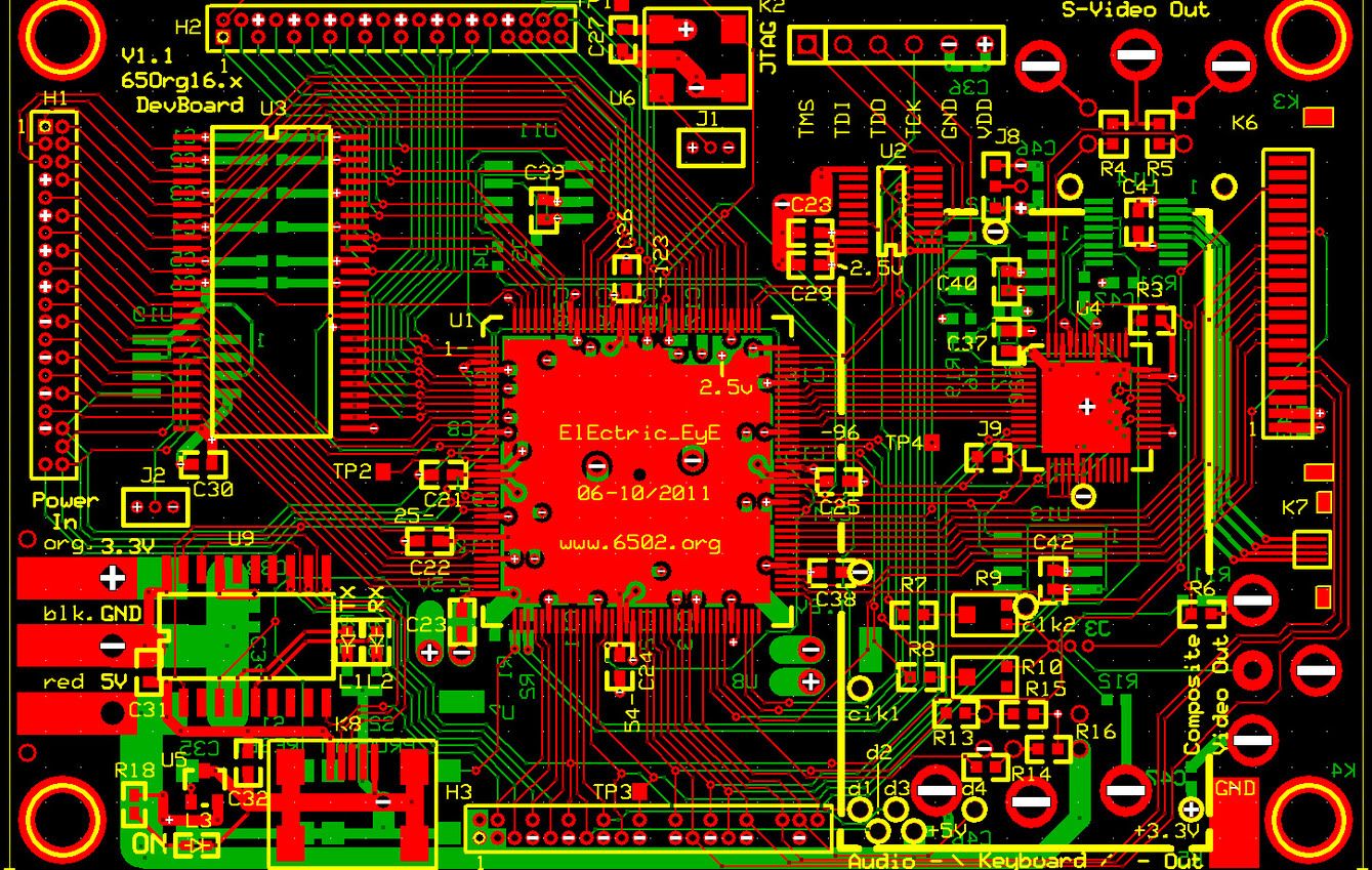
Here is the V1.1 DevBoard Schematic.
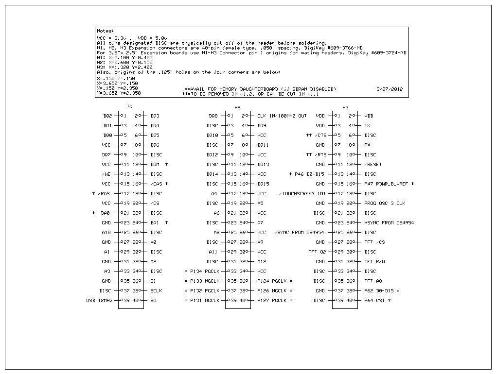
Here is the pinout for the expansion Headers.

EDIT (12/17/2011): Added parts list per request. Initial post, incomplete...
EDIT (1/7/2012): Added Memory Map
EDIT (1/17/2012): Added Random Number Generator to Memory Map.
EDIT (1/20/2012): Added Board Layout and Schematic.
EDIT (3/27/2012): Added updated Header info. NOTE: Header pinouts are not up to date on Schematic.
Last edited by ElEctric_EyE on Tue Mar 27, 2012 2:10 pm, edited 7 times in total.
User avatar
BigEd
Posts: 11463
Joined: 11 Dec 2008
Location: England
Contact:

Post by BigEd »

Hi EEye
could we have a link to your v1.1 layout please?
Ta
Ed
ElEctric_EyE
Posts: 3260
Joined: 02 Mar 2009
Location: OH, USA

Post by ElEctric_EyE »

BigEd wrote:
Hi EEye
could we have a link to your v1.1 layout please?
Ta
Ed
Sure, here it is. It should be updated to the final tonight, but what you see in the link now is next to the last "progression", i.e. I had 15 progressions before V1.1 was completed. (1 via was switched from H1 to near U13, and labelling is different for audio.). I was really starting to go off on a tangent for the audio. In the end I think the sound board will be a daughterboard utilizing the 3 Headers, and not just the pins as I have them labelled.
User avatar
BigEd
Posts: 11463
Joined: 11 Dec 2008
Location: England
Contact:

Post by BigEd »

Thanks! I was a bit confused because this 144-lead FPGA looks on your photos like it has only 72 leads - must be just because they can't show the detail. Soldering at 0.5mm pitch wasn't too bad?
ElEctric_EyE
Posts: 3260
Joined: 02 Mar 2009
Location: OH, USA

Post by ElEctric_EyE »

I had used 640x480 for the camera for small pictures. I got some decent detail with the closeup on the first pic though, despite the low res...

As far as soldering, as what's been said before in other parts of the forum and the internet, using flux is critical. I use a needle like dispenser with a fine point. I used no solder at all on the FPGA. The flux allows you to see the solder flow underneath each pin.
What has not been mentioned so much is the condition of the eyesight of the one doing the soldering work! I am extremely near-sighted, so when I do my soldering without my glasses, I see it very clear about 2-3in from my eyes. When I do need magnification when things are suspected short, I use clip-on lenses with my glasses. Talk about eye strain!
User avatar
BigEd
Posts: 11463
Joined: 11 Dec 2008
Location: England
Contact:

Post by BigEd »

Very good point - that first picture makes it clear.

I'm about as near-sighted as you are. I haven't tried anything as fine as that. Yet. I'm not sure I want unprotected eyes quite so close, but I have a couple of magnifiers. Anyway, as you say, soldering topics have been covered elsewhere.

I suppose you're some way from trying to bring the RAM to life?

Cheers
Ed
ElEctric_EyE
Posts: 3260
Joined: 02 Mar 2009
Location: OH, USA

Post by ElEctric_EyE »

BigEd wrote:
...I suppose you're some way from trying to bring the RAM to life?

Cheers
Ed
Hopefully Arlet will lead the way there when it comes time, which shouldn't be too long, I hope. I know he has mentioned the speed of the SDRAM may have to run 2x faster than the CPU for some configurations?, IIRC. I could use the PLLs for this, there is one left. I really would like to get the I2C working so I can put the DS1085LZ-5 frequency generators to work for this, and save the last PLL.
User avatar
Arlet
Posts: 2353
Joined: 16 Nov 2010
Location: Gouda, The Netherlands
Contact:

Post by Arlet »

If you want maximum performance, you could run the SDRAM faster than the CPU, but for simplicity, I'd recommend running both at the same speed to start with. It also depends on the max speed. If the SDRAM is limited to 133MHz, and the CPU to 100 MHz, there's not much point in letting the SDRAM run faster.
ElEctric_EyE
Posts: 3260
Joined: 02 Mar 2009
Location: OH, USA

Post by ElEctric_EyE »

I did get the 167MHz higher speed grade SDRAM. But right now the CPU is running off of the 27MHz pixel clock.
User avatar
Arlet
Posts: 2353
Joined: 16 Nov 2010
Location: Gouda, The Netherlands
Contact:

Post by Arlet »

ElEctric_EyE wrote:
I did get the 167MHz higher speed grade SDRAM. But right now the CPU is running off of the 27MHz pixel clock.
It's fairly easy to have a pixel clock that's completely different than the CPU or memory clock, because data only goes one way. It's just a matter of putting an asynchronous FIFO in the path. Data goes into the FIFO on the fast clock, and out of the FIFO with the pixel clock. When the FIFO is near empty, you start another memory burst to fetch some more data, and you stop the burst when the FIFO is full.

It's trickier to put the SDRAM and the CPU on different clocks, especially if they aren't a simple ratio, like 1:2.
ElEctric_EyE
Posts: 3260
Joined: 02 Mar 2009
Location: OH, USA

Post by ElEctric_EyE »

Arlet wrote:
...It's fairly easy to have a pixel clock that's completely different than the CPU or memory clock, because data only goes one way. It's just a matter of putting an asynchronous FIFO in the path. Data goes into the FIFO on the fast clock, and out of the FIFO with the pixel clock. When the FIFO is near empty, you start another memory burst to fetch some more data, and you stop the burst when the FIFO is full.

It's trickier to put the SDRAM and the CPU on different clocks, especially if they aren't a simple ratio, like 1:2.
I think I understand if we were to use this memory as video memory.
The output of the FIFO goes to the video shift register, in this case a CS4954 and is clocked at the pixel rate.
Data is written to the FIFO from the SDRAM in bursts. After the FIFO is full, the SDRAM is free and can be read/written to by the CPU. To keep things simple, CPU and SDRAM are running at the same speeds, let's say 50MHz. At this point does the cpu change the burst length in order to use the RAM like ordinary SRAM? so it can RMW single video memory locations?
User avatar
Arlet
Posts: 2353
Joined: 16 Nov 2010
Location: Gouda, The Netherlands
Contact:

Post by Arlet »

ElEctric_EyE wrote:
I think I understand if we were to use this memory as video memory.
The output of the FIFO goes to the video shift register, in this case a CS4954 and is clocked at the pixel rate. Data is written to the FIFO from the SDRAM in bursts. After the FIFO is full, the SDRAM is free and can be read/written to by the CPU.
What I would do is make an SDRAM controller with 2 ports, one port for the video output FIFO, and another port for the CPU, so both CPU and video generator can request access to the SDRAM. The SDRAM controller also contains an arbiter block, who's task it is to choice between the two devices.

For instance:

If the CPU is doing a burst, and the video FIFO still holds more than N bytes, we can let the CPU continue.

If the CPU is doing a burst, and video FIFO holds less than N bytes, abort the CPU burst, and start a video access.

If video is busy, and FIFO holds less than M bytes, we let video continue.

If video is busy, FIFO holds more than M bytes, and CPU requests , stop video burst, and start CPU access.

If video is busy, and CPU does not request bus, continue until video FIFO is full.

It may sound complicated, but each of those tests is just one line in verilog.

It's also possible to implement a DMA controller as a 3rd port to the SDRAM interface. Because the 6502 CPU and 65Org16 derivatives don't have a natural burst method, you can make a separate hardware state machine that will copy a block of SDRAM data into a block RAM, and give the CPU access to the other side of the block RAM.

This would work like so:

- CPU writes start address and length into DMA controller registers
- DMA controller copies data block from block RAM to SDRAM, or vice versa
- when DMA controller is ready, the CPU gets an interrupt, or can poll a status bit.
- CPU gets direct access to block RAM to read/write the data.
ElEctric_EyE
Posts: 3260
Joined: 02 Mar 2009
Location: OH, USA

Post by ElEctric_EyE »

Some excellent information!
Your "IF" statements don't sound too complicated... When doing my ORs module, the error messages and synthesis warnings actually led me in the right direction, along with some google searches. From looking at others' code I could gather the general syntax...

Just a question, right off the top:

How big of a FIFO buffer would have to be used do you think at the speeds mentioned? and..
It would have to be inside the FPGA no doubt as block ram?

Regarding the second half of your statement about DMA:
Arlet wrote:
...and give the CPU access to the other side of the block RAM.
..
You mean the other side of the SDRAM, not the block ram right? Because, since the video shift register is only 8-bits wide and the SDRAM is 16-bits wide, half of the memory is unused!

P.S. The board layout link has been updated and now reflects 100% what is seen in the pics.
User avatar
Arlet
Posts: 2353
Joined: 16 Nov 2010
Location: Gouda, The Netherlands
Contact:

Post by Arlet »

ElEctric_EyE wrote:
How big of a FIFO buffer would have to be used do you think at the speeds mentioned? and.. It would have to be inside the FPGA no doubt as block ram?
Yes, a block RAM. And you'd use the whole thing, so when the CPU is doing something else, you can read long bursts for the video.
Quote:
You mean the other side of the SDRAM, not the block ram right? Because, since the video shift register is only 8-bits wide and the SDRAM is 16-bits wide, half of the memory is unused!
The block RAMs inside the FPGA can have different widths on both sides. So, you'd have a block RAM with 16 bit input from SDRAM, and 8 bit output to video shift.
ElEctric_EyE
Posts: 3260
Joined: 02 Mar 2009
Location: OH, USA

Post by ElEctric_EyE »

Arlet wrote:
Yes, a block RAM. And you'd use the whole thing, so when the CPU is doing something else, you can read long bursts for the video...
This pretty much means this Spartan 6 would be dedicated for video. I was using block RAMs for zero page, stack and ROM for the 65Org16.
Arlet wrote:
..The block RAMs inside the FPGA can have different widths on both sides. So, you'd have a block RAM with 16 bit input from SDRAM, and 8 bit output to video shift.
How does that work? Does it just truncate a byte?
Post Reply