A 6502 SoC Project using a Spartan 3 FPGA
-
ElEctric_EyE
- Posts: 3260
- Joined: 02 Mar 2009
- Location: OH, USA

You can also use the built-in Isim simulation in the ISE program.
In the ISE Design tab, there are buttons to choose between 'Implementation' and 'Simulation'. If you click on 'Simulation', you can highlight the top level schematic, and simulate it.
You'll need a create a small test bench, though. A simple clock, plus a reset pulse is enough to get started.
In the ISE Design tab, there are buttons to choose between 'Implementation' and 'Simulation'. If you click on 'Simulation', you can highlight the top level schematic, and simulate it.
You'll need a create a small test bench, though. A simple clock, plus a reset pulse is enough to get started.
-
ElEctric_EyE
- Posts: 3260
- Joined: 02 Mar 2009
- Location: OH, USA
I'll be sure to check ISim out first. Give me 2 days (tue,wed) when I can dedicate 2 full consecutive days to get some results. I also need to check the current timing reports for stated delays...
In the meantime, I would like to pose a question about modifying your core for a few very basic 65C02 clock saving instructions. Instructions like PHX, PHY, PLX, PLY, STZ, and TXY, TYX. I'm a novice 65C02 programmer (experienced MOS 6502), but these are the instructions I've intuitively understood, although TXY and TYX are native to the 65816. If you were to ask a programmer of the original 6502 what these instructions meant, he would know immediately.
What are your thoughts on this? In your opinion, how much effort would be involved for a HDL/Verilog coder to mod your core for these instructions?
-
ElEctric_EyE
- Posts: 3260
- Joined: 02 Mar 2009
- Location: OH, USA
I tried ISim today. Had difficulty creating a testbench where I could input a O2 frequency and control a reset.
I spent a good deal of time on my 20MHz 65C02 proof(PWA) today just to make sure I had the same 6502 code for it, as inside the 6502SoC. The proof is up and running with the same software as the 6502SoC at this point, except for the RAM banking and EEPROM to SRAM copy.
And at this point, the 6502SoC with the main clock @45MHz, nothing runs, the display doesn't even try to init. When I divide the main clock by 2, for 22.5MHz, the display clears after alot of wrong data, almost like the display is receiving correct data, but A0 is changing, thereby changing display characteristics. When the main clock is divided by 4, for 11.25MHz, it works almost flawlessly. I think tomorrow I will focus on A0 delays.
I am trying to learn about timing constraints and manipulate the text file generated by the constraints editor.
Now I have a single .UCF file where pin assignments and bank voltages were made using PlanAhead, and below a few lines made by using the Timing Constraints App. Still experimenting...
Observations:
1) The /PROGRAM button does work 100%. The faster speeds were locking the system up. After lowering main clock speeds to 11.25MHz, it works fine.
2) The post simulation max speed for this design was 53MHz.
3) Max delay from O2 to pad was ~9ns.
4) Reset is touchy like it needs debouncing, maybe a simple cap/resister.
5) NMI (RES2) interrupt switch works every time, much less susceptible to bounce. Interesting to note as well, action is not taken until the NMI button is released.
I spent a good deal of time on my 20MHz 65C02 proof(PWA) today just to make sure I had the same 6502 code for it, as inside the 6502SoC. The proof is up and running with the same software as the 6502SoC at this point, except for the RAM banking and EEPROM to SRAM copy.
And at this point, the 6502SoC with the main clock @45MHz, nothing runs, the display doesn't even try to init. When I divide the main clock by 2, for 22.5MHz, the display clears after alot of wrong data, almost like the display is receiving correct data, but A0 is changing, thereby changing display characteristics. When the main clock is divided by 4, for 11.25MHz, it works almost flawlessly. I think tomorrow I will focus on A0 delays.
I am trying to learn about timing constraints and manipulate the text file generated by the constraints editor.
Now I have a single .UCF file where pin assignments and bank voltages were made using PlanAhead, and below a few lines made by using the Timing Constraints App. Still experimenting...
Code: Select all
NET "O2" TNM_NET = O2;
TIMESPEC TS_O2 = PERIOD "O2" 22 ns HIGH 50% INPUT_JITTER 100 ps;
NET "O2Out" OFFSET = OUT 9.5 ns AFTER "O2" FALLING;
1) The /PROGRAM button does work 100%. The faster speeds were locking the system up. After lowering main clock speeds to 11.25MHz, it works fine.
2) The post simulation max speed for this design was 53MHz.
3) Max delay from O2 to pad was ~9ns.
4) Reset is touchy like it needs debouncing, maybe a simple cap/resister.
5) NMI (RES2) interrupt switch works every time, much less susceptible to bounce. Interesting to note as well, action is not taken until the NMI button is released.
-
ElEctric_EyE
- Posts: 3260
- Joined: 02 Mar 2009
- Location: OH, USA
I don't know why I kept thinking 45MHz as the default frequency of the DS1085-5. It's 48.58MHz. So rewriting the constraint below (after some other fiddling) worked @ 24MHz! I always seem to have the greatest success in the mornings. . Now if I can get the display to run @48MHz, I will be very happy indeed.
---------------------------------------------------------------------------------------------------------------------------------------------------------------------------------------------------------------------------------------------------------------------------
I was abit premature in my declaration of success 7 hrs ago. I later realized I had a timing constraint error because my 5.5ns "estimated" delay is shorter than the internal delay (as spec'd by ISE), from O2 to pad, of 11.7ns. Although the circuit still worked the best I had so far, it was locking up after some time (<1min)...
After looking over some of my old schematics from the PWA project, I decided to qualify WE from Arlet's 6502 core with O2/2. In addition, instead of an arbitrary 5.5ns, I calculated the actual time I needed to put O2Out in sync with O2, although the display likes an inverted version of O2.
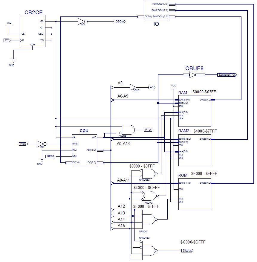
The 6502SoC has been running now for over an hour with no problems @24MHz using this constraint with the schematic below:
As I am not a timing diag kind of person, I realized in the middle of posting this, that the diagram below is incorrect. The 2 waveforms below O2 are divided by 2 in the schematic. As usual with me, I happen across my successes sometimes by accident. This "accident" will give me insight to pushing for 48MHz, because for sh*ts and giggles I just now tried to run the 6502SoC @48MHz, and it cleared the display. Although repeatability was not there yet, it did more now than previous attempts @48MHz... I'm zeroing in!
Updated schematic:
Note(s) to self: After reading this post on my 2nd favorite forum, Xilinx forums, Austin Lesea (their principle engineer) comments on jitter value ranges. "...100ps for synchronous design with single clock...", and "...1000ps for... poor bypassing...".
A video about switch debouncing an FPGA.
A video about someone with similar ideas to mine using an XC3S400, T65 core, PS/2 interface, and an SDCard interface. Darn I though I would've been the only one, heh!, I'm always behind the power curve... I asked on his video what speed he is running the T65 core. Waiting for response, doubt I'll get any, been posted a year ago...
Code: Select all
NET "O2" TNM_NET = O2;
TIMESPEC TS_O2 = PERIOD "O2" 20.5 ns HIGH 50% INPUT_JITTER 100 ps;
NET "O2Out" OFFSET = OUT 5.5 ns AFTER "O2" RISING;
I was abit premature in my declaration of success 7 hrs ago. I later realized I had a timing constraint error because my 5.5ns "estimated" delay is shorter than the internal delay (as spec'd by ISE), from O2 to pad, of 11.7ns. Although the circuit still worked the best I had so far, it was locking up after some time (<1min)...
After looking over some of my old schematics from the PWA project, I decided to qualify WE from Arlet's 6502 core with O2/2. In addition, instead of an arbitrary 5.5ns, I calculated the actual time I needed to put O2Out in sync with O2, although the display likes an inverted version of O2.
The 6502SoC has been running now for over an hour with no problems @24MHz using this constraint with the schematic below:
Code: Select all
NET "O2" TNM_NET = O2;
TIMESPEC TS_O2 = PERIOD "O2" 20.5 ns HIGH 50% INPUT_JITTER 100 ps;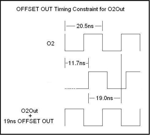
NET "O2Out" OFFSET = OUT 19.0 ns AFTER "O2" RISING;Updated schematic:
Note(s) to self: After reading this post on my 2nd favorite forum, Xilinx forums, Austin Lesea (their principle engineer) comments on jitter value ranges. "...100ps for synchronous design with single clock...", and "...1000ps for... poor bypassing...".
A video about switch debouncing an FPGA.
A video about someone with similar ideas to mine using an XC3S400, T65 core, PS/2 interface, and an SDCard interface. Darn I though I would've been the only one, heh!, I'm always behind the power curve... I asked on his video what speed he is running the T65 core. Waiting for response, doubt I'll get any, been posted a year ago...
-
ElEctric_EyE
- Posts: 3260
- Joined: 02 Mar 2009
- Location: OH, USA
Arlet wrote:
...but if you're only writing to the display, it shouldn't matter.
I did take ISE In-Depth tutorial and the laptop with ISE 12.3 and the 6502SoC project file. I had intentions of learning about testbenches, but I came across a debounce circuit in verilog and VHDL and how to implement it in a design on (Pg.23 to Pg. 28).
I followed the directions, but I'm getting an error. I think I'm putting a semicolon in the wrong spot. I really have no clue of proper syntax. Help?
Code: Select all
library IEEE;
use IEEE.STD_LOGIC_1164.ALL;

entity debounce is
    Port ( sig_in : in  STD_LOGIC;
           clk : in  STD_LOGIC;
           sig_out : out  STD_LOGIC);
end debounce;

architecture Behavioral of debounce is

signal Q1, Q2, Q3 : STD_LOGIC;

begin

process (<clk>)
begin
   if (<clk>'event and <clk> = '1') then
         Q1 <= sig_in;
         Q2 <= Q1;
         Q3 <= Q2;
	end if;
end process;

sig_out <= Q1 and Q2 and (not Q3);

end Behavioral;
ERROR:HDLParsers:164 - "C:/a/debounce.vhd" Line 41. parse error, unexpected IF, expecting SEMICOLON
Last edited by ElEctric_EyE on Sun Mar 06, 2011 7:46 pm, edited 1 time in total.
-
ElEctric_EyE
- Posts: 3260
- Joined: 02 Mar 2009
- Location: OH, USA
One thing I noticed that you have:
and that the example has:
Not sure if that makes a difference.
Code: Select all
signal Q1, Q2, Q3 : STD_LOGIC;Code: Select all
signal Q1, Q2, Q3 : std_logic;ElEctric_EyE wrote:
Code: Select all
process (<clk>)
begin
   if (<clk>'event and <clk> = '1') then
         Q1 <= sig_in;
         Q2 <= Q1;
         Q3 <= Q2;
	end if;
end process;
ERROR:HDLParsers:164 - "C:/a/debounce.vhd" Line 41. parse error, unexpected IF, expecting SEMICOLON
Identifiers in VHDL are not case sensitive, so it doesn't matter if you write "std_logic" or "STD_LOGIC".
so long,
Hias
From the tutorial. See 6c.
Quote:
6. VHDL only: Complete the VHDL module by doing the following:
a. Move the line beginning with the word signal so that it is between the
architecture and begin keywords.
b. Remove the reset logic (not used in this design) by deleting the five lines beginning with if (<reset>... and ending with else, and delete one of the end if;
lines.
c. Change <clock> to clk; D_IN to sig_in; and Q_OUT to sig_out. Note: You can select Edit > Find & Replace to facilitate this. The Find fields appear at the bottom of the Text Editor.
-
ElEctric_EyE
- Posts: 3260
- Joined: 02 Mar 2009
- Location: OH, USA
-
ElEctric_EyE
- Posts: 3260
- Joined: 02 Mar 2009
- Location: OH, USA
Made the symbol and put it in the schematic. Tried to wire it up, but it wouldn't connect.
I right clicked on the symbol in the schematic to edit it. Added pins for sig_in, clk, and sig_out. Now it connects ok. I went back to the vhdl file, expecting ISE to have modified it in some way for having added I/O pins, but it didn't...Anyway,
I copied the debounce.vhd file from the laptop to the desktop that's physically connected to the 6502SoC. Right clicked in Hierarchy to add source and added debounce.vhd. Created the debounce symbol and connected it to the inverter before RES (Reset) and RES2 (NMI) in the schematic, using O2/2 as the clk for the debounce symbols. Now nothing works.
Any input appreciated, I'm off now to give the brain a rest until tue&wed.
ElEctric_EyE wrote:
Created the debounce symbol and connected it to the inverter before RES (Reset) and RES2 (NMI) in the schematic, using O2/2 as the clk for the debounce symbols. Now nothing works.
I don't know the logic behind your RES and NMI inputs, but this might not be the kind of signal you are expecting.
If you want to protect the circuit against single-cycle spikes you could, for example, add a "best-of-3" decoder: The output is high if the input was high for 2 or 3 cycles, otherwise it's low (if the input was low for 2 or 3 cycles).
The logic is quite simple:
Code: Select all
sig_out <= (Q1 and Q2) or (Q1 and Q3) or (Q2 and Q3);Code: Select all
   if (<clk>'event and <clk> = '1') then
         Q0 <= sig_in;
         Q1 <= Q0;
         Q2 <= Q1;
         Q3 <= Q2;
end if;so long,
Hias