6502.org Forum  Projects  Code  Documents  Tools  Forum
It is currently Mon Apr 29, 2024 6:33 am

All times are UTC


Post new topic Reply to topic  [ 224 posts ]  Go to page 1, 2, 3, 4, 5 ... 15  Next
Author Message
PostPosted: Tue Jan 04, 2011 3:57 am 
Offline

Joined: Mon Mar 02, 2009 7:27 pm
Posts: 3258
Location: NC, USA
I've had success recently fitting a PS2 keyboard core into the smallest of the Spartan 2 FPGA's: the 100-pin QFP XC2S15.

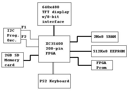
In this thread I would like to attempt at fitting a few more "cores" into a larger Xilinx FPGA, the Spartan 3!:

1) Arlet's 6502 Core
2) A PS2 keyboard interface core
3) An I2C core

4) A USB or SD card Core

All the cores are written in HDL or Verilog. Most will be obtained from opencores.org. I will use a top-level schematic to connect them all. I know the PS2/I2C cores have wishbone I/O interfaces. Will have to search out USB/SD card...

I have graphic software routines, controlled by the PS2 interface, that I've written for my W65C02 controlled PWA project, and would like for them not to go to waste, since I have decided to take advantage of 65816 to replace the 6502 in that project. The routines are meant for a 5.7" 640x480 TFT/LCD NewHaven display. It has an 8-bit display controller built in, which supposedly can run to 50+MHz.

So I thought, this is the perfect time to start this thread. Certain pieces have fell into place to finalize my decisions about the next major step of progress with the PWA, i.e. I've decided to use the 65816. The last piece of software has to be completed for the 6502PWA project is a memory hex dump routine, which I intend to use here as well.

I'll be posting everything: hardware & software here. So you can grill my weak software skills. :lol:

Anticipated completion for this "6502SoC" project is 6 months to 1 yr. The goal is simply to use all the Cores with the graphic routines, and of course to see top speed of Arlet's 6502! More details will be exposed, as the thread continues...

Edit: Renamed title. Clarified further.

_________________
65Org16:https://github.com/ElEctric-EyE/verilog-6502


Last edited by ElEctric_EyE on Tue Jan 04, 2011 12:34 pm, edited 3 times in total.

Top
 Profile  
Reply with quote  
 Post subject:
PostPosted: Tue Jan 04, 2011 9:53 am 
Offline
User avatar

Joined: Thu Dec 11, 2008 1:28 pm
Posts: 10793
Location: England
Hi EEye
this should be an interesting adventure! However, I'd say that 'multi-core' means more than one CPU, so this is better described as a 'system on chip' or similar. I recommend you rename your post before too many people get too excited about the possibility of multi-processing on an FPGA (which is surely also possible, but isn't what you're about to do)

How about 6502SOC?

Cheers
Ed


Top
 Profile  
Reply with quote  
 Post subject:
PostPosted: Tue Jan 04, 2011 11:30 am 
Offline
User avatar

Joined: Tue Nov 16, 2010 8:00 am
Posts: 2353
Location: Gouda, The Netherlands
How are you producing the graphics ? I didn't see a VGA module on your list, and I didn't really understand the reference to PS2 with respect to the graphics software. Do you have a link to your earlier work ?

BTW, I agree with Ed regarding the terminology.


Top
 Profile  
Reply with quote  
 Post subject:
PostPosted: Tue Jan 04, 2011 12:57 pm 
Offline
User avatar

Joined: Thu Dec 11, 2008 1:28 pm
Posts: 10793
Location: England
I think this kind of LCD display has internal frame buffer storage, so the system just sits on the bus, occupying 2 addresses, and the CPU reads and writes to the port to write pixels into it. No VGA port needed (and no frame buffer or video signal generator)

For lower performance but a simpler interface, the display could probably be driven by a PIA or VIA kind of port (it has 8 data lines and about 4 control lines, plus reset and some mode inputs) - see the spec (PDF)

Anyhow, EEye has been pursuing a system like this in his (20-page!)
Project: Digital Fuel Injector Pulse Width Analyzer thread


Top
 Profile  
Reply with quote  
 Post subject:
PostPosted: Tue Jan 04, 2011 1:15 pm 
Offline

Joined: Mon Mar 02, 2009 7:27 pm
Posts: 3258
Location: NC, USA
I agree, if I first read "6502 Multi-Core..", I would've thought that too.

Arlet wrote:
How are you producing the graphics ? I didn't see a VGA module on your list, and I didn't really understand the reference to PS2 with respect to the graphics software...


No VGA core, yet. I really wanted to keep everything moderately simple. Simple is fast. Besides connecting multiple I/O cores onto an FPGA, one of the main goals is to see top speed of your CPU design. Although, after refreshing my memory, and rereading BigEd's post after you added BCD mode here, I see the expected speed @~54MHz. That will go perfectly with the SSD1963, as that top speed is ~50MHz. Should make for some impressive 6502 controlled graphics methinks!

So I am relying on a hardware controlled TFT display for the video. It's a 640x480 pixel display with 18-bit color. I will have to explain abit more about the controller later, it's very nice. But for anyone interested it's an SSD1963.

I have 2 fonts, 3x5 & C-64. I use only 16 colors, same colors as the C-64, in a lookup table. Also, there are 7 sizes. These are the character attributes.

When you type on the keyboard, you see the characters. This much I've accomplished.

I'm working on the last piece of 6502 software for my PWA project in the hardware section. It is a hex dump from a banked 2Mx8 SRAM to the display. That PWA project is going to morph into a 65816 controlled system. I'll update that thread soon as well...

But as I said, I didn't want this effort into the software to be wasted, so what better way to use a known successful chunk of software to test the 6502SoC, especially since it is already using 1 of the I/O interfaces.

Earlier I said, this could take 6 months to a year. I don't anticipate getting the 6502 core and the PS2 core "up and running" to take very long, after the wiring.

Nothing is even on paper yet, but my little mind's eye is picturing 5 IC's:

The XC3S400 Spartan 3
The FPGA PROM
A 2Mx8 SRAM
A 512Kx8 EEPROM
An I2C programmable oscillator

Here's a block diag of what I'm thinking. As in the PWA, the "OS" will be copied from slow EEPROM @F1(2.5MHz), and run from SRAM @F2(20MHz+). The 2GB SD will hold "test data". I'm thinking bitmap pic info that can be readily copied from the PC to the SD card. Then plugged into 6502SoC and outputted to the display to test the SD core.
Image

CPU core chosen. I'll list and credit the other cores next...

edit: Added more info after, "No VGA yet,..."

_________________
65Org16:https://github.com/ElEctric-EyE/verilog-6502


Last edited by ElEctric_EyE on Tue Jan 04, 2011 10:49 pm, edited 1 time in total.

Top
 Profile  
Reply with quote  
 Post subject:
PostPosted: Tue Jan 04, 2011 5:28 pm 
Offline
User avatar

Joined: Tue Nov 16, 2010 8:00 am
Posts: 2353
Location: Gouda, The Netherlands
Well, if you're interested, I don't think it would be too hard to add a VGA interface directly in the FPGA. I already have some verilog lying around from some earlier projects that I could clean up and donate. See below for a picture of my spartan-3 eval board, hooked up to a test board with a QVGA panel, showing some test font.

The frame buffer is stored in an SRAM chip (included on spartan-3 board). The SRAM interface ran at 100 MHz, but the pixel clock was only 25 MHz. I only had a simple state machine instead of a CPU to write the data. It would be an option to raise the pixel clock to 50 MHz, which would allow something like 800x600, combined with a 50 MHz 6502, alternating access cycles on the SRAM.

Lower speeds are possible too, of course.

ETA: advantage of a home-built VGA controller is that you can implement different color modes, or implement some 2D acceleration features like a bit blit.

Image


Top
 Profile  
Reply with quote  
 Post subject:
PostPosted: Tue Jan 04, 2011 6:07 pm 
Offline
User avatar

Joined: Thu Dec 11, 2008 1:28 pm
Posts: 10793
Location: England
(skipping over Arlet's interesting VGA story and kind offer...)

On the boot rom front, it would be tempting to ditch the conventional EEPROM and use an i2c EEPROM - 256kbit for $2 especially if you have an i2c port already, and an SD card interface nearby. The EEPROM only has to contain a bootstrap which should be small and stable, just enough to load application or OS code from SD. Actually if the bootstrap is small enough you could place it inside the FPGA, which is even simpler.


Top
 Profile  
Reply with quote  
 Post subject:
PostPosted: Tue Jan 04, 2011 6:30 pm 
Offline
User avatar

Joined: Tue Nov 16, 2010 8:00 am
Posts: 2353
Location: Gouda, The Netherlands
BigEd wrote:
Actually if the bootstrap is small enough you could place it inside the FPGA, which is even simpler.


Yes, there's plenty of room inside the block RAMs, and you can preload them with code, use as a bootloader, and afterwards use them as regular RAM.


Top
 Profile  
Reply with quote  
 Post subject:
PostPosted: Tue Jan 04, 2011 7:42 pm 
Offline

Joined: Mon Mar 02, 2009 7:27 pm
Posts: 3258
Location: NC, USA
All in good time my friends. I'm not as advanced as you guys might think! I have to start from a 'known' foundation. However, it's nice to throw ideas out there, so I will do the same.

As far as VGA, looking at some of the cheapest LCD monitor prices on newegg.com, it may be worth looking into as it would be more universal.

I've seen some HDL code for a VGA controller on FPGA4Fun website, and it looked pretty short. Not sure how to interface it to the 6502 though? What about your code Arlet? I could use the display I'm now using for development purposes, and have the VGA part as an add-on later...

I haven't tested I2C core yet, so I need to start small with that DS1085 programmable freq. generator. As far as RAM though, how much block ram would be available? Maybe I could get rid of the external 2Mx8 SRAM?

(Drank too much coffee this morning and my brain is fizzled out, so I can't even finish up my hex dump software)

_________________
65Org16:https://github.com/ElEctric-EyE/verilog-6502


Top
 Profile  
Reply with quote  
 Post subject:
PostPosted: Tue Jan 04, 2011 8:30 pm 
Offline
User avatar

Joined: Tue Nov 16, 2010 8:00 am
Posts: 2353
Location: Gouda, The Netherlands
The XC3S400 you mention has 16 block RAMs of 2KB each. Each block RAM is a dual ported memory, and can be configured as 9, 18, or 36 bits wide. You can combine multiple blocks to make deeper or wider RAMs.

If you want on-board VGA controller, you'll need external SRAM for graphics frame buffer. If you just want text, you can run VGA from block RAM. Here's one of my very first projects with my Spartan-3 eval board, using 2 block RAMs. One for text buffer, the other for character ROM: http://ladybug.xs4all.nl/arlet/fpga/text2.jpg, because all block RAMs are dual ported, the other port is free for easy CPU access.

With my graphics version of the VGA controller, the data comes from external SRAM, and the 6502 can write to same SRAM. This is done with a dual port SRAM controller. From the 6502's perspective, part of the memory map would be mapped to the video memory. As you store data in that memory, it'll show up directly on the screen.

What kind of hardware are you planning to use ? Some standard FPGA board, or something home made ?


Top
 Profile  
Reply with quote  
 Post subject:
PostPosted: Tue Jan 04, 2011 9:23 pm 
Offline

Joined: Mon Mar 02, 2009 7:27 pm
Posts: 3258
Location: NC, USA
Arlet wrote:
The XC3S400 you mention has 16 block RAMs of 2KB each...


I didn't think it would have been that limited. The SSD1963 LCD controller has 1.2MB of built in RAM. I'm sure it's some sort of FPGA. It's only 144-pin QFP... But anyway, that scraps the VGA idea. Only because I intend to eventually have 4-layer 3.5"x2.8" mini-pro boards made by ExpressPCB. So chip count needs to be as low as possible at this point.

Arlet wrote:
...What kind of hardware are you planning to use ? Some standard FPGA board, or something home made ?


Home made using wirewrap. I already experimented soldering the XC3S400 208-pin QFP using a PGA adapter and wire wrap headers. Been sitting on an anti-static pad gathering dust!

Edit: Corrected BGA to PGA!

_________________
65Org16:https://github.com/ElEctric-EyE/verilog-6502


Last edited by ElEctric_EyE on Tue Jan 04, 2011 11:11 pm, edited 1 time in total.

Top
 Profile  
Reply with quote  
 Post subject:
PostPosted: Tue Jan 04, 2011 9:45 pm 
Offline

Joined: Sat Jan 04, 2003 10:03 pm
Posts: 1706
The LCD panel probably has a custom ASIC which is made from standard cores found on FPGAs. I know, when I worked at Hifn, our engineers used Verilog to design ASICs using a lot of the same cores as were found in FPGA libraries.

I don't know any of the details on how they did this though, as I worked in a different department (I was post-silicon, not pre-silicon).


Top
 Profile  
Reply with quote  
 Post subject:
PostPosted: Wed Jan 05, 2011 9:40 am 
Offline
User avatar

Joined: Tue Nov 16, 2010 8:00 am
Posts: 2353
Location: Gouda, The Netherlands
ElEctric_EyE wrote:
Home made using wirewrap. I already experimented soldering the XC3S400 208-pin QFP using a PGA adapter and wire wrap headers. Been sitting on an anti-static pad gathering dust!


Ok, well, I may still work on this stuff when I have some free time. My goal would be something that runs on a simple FPGA eval board, and that has a 6502 core, video output, keyboard input, and whatever seems useful, so it can be used as basis for other projects.


Top
 Profile  
Reply with quote  
 Post subject:
PostPosted: Wed Jan 05, 2011 9:24 pm 
Offline

Joined: Mon Mar 02, 2009 7:27 pm
Posts: 3258
Location: NC, USA
I have the same desire, but wish to make custom boards in the end, and save money by not purchasing an eval board.

Couple questions though...

Which version of Spartan 3 is on your eval board?
What kind of eval board do you have?

_________________
65Org16:https://github.com/ElEctric-EyE/verilog-6502


Top
 Profile  
Reply with quote  
 Post subject:
PostPosted: Wed Jan 05, 2011 9:27 pm 
Offline
User avatar

Joined: Thu Dec 11, 2008 1:28 pm
Posts: 10793
Location: England
Would it be good to have a thread with a first post which tabulates various dev boards, with links and price and maybe some indication of capability?

A bit like the 6502 FPGA core thread...

Of course it would need revisiting once or twice a year as things change, but if it carries a date that's no problem.

Cheers
Ed

Edit: oops, mistyped 6502 and caused a Terbium fest


Last edited by BigEd on Wed Jan 05, 2011 10:17 pm, edited 1 time in total.

Top
 Profile  
Reply with quote  
Display posts from previous:  Sort by  
Post new topic Reply to topic  [ 224 posts ]  Go to page 1, 2, 3, 4, 5 ... 15  Next

All times are UTC


Who is online

Users browsing this forum: No registered users and 11 guests


You cannot post new topics in this forum
You cannot reply to topics in this forum
You cannot edit your posts in this forum
You cannot delete your posts in this forum
You cannot post attachments in this forum

Search for:
Jump to: