6502 Timing Controls: T0?

Let's talk about anything related to the 6502 microprocessor.
Xor
Posts: 19
Joined: 10 Jan 2011

6502 Timing Controls: T0?

Post by Xor »

What, in the 6502, drives T0 low? With my own fumbling I've been unable to deduce the logic that drives T0 low. I've mostly figured out the other tcstate bits:

Code: Select all

tcstate[1] <= tcstate[0];

if(rdy0)
     tcstate[5:3] <= 3'b111;
else
     tcstate[5:3] <= tcstate[4:2];

tcstate[2] <= !sync;
sync is controlled by some fetch flip-flop, and fetch is controlled by tcstate[0].

As far as I can tell, T0 is driven high after PLA34 is high (which goes high when T0 goes low). i.e.

Code: Select all

assign pla[34] = !tcstate[0];

if(pla[34]) tcstate[0] <= 1'b1;
However, I don't know what drives it low. It seems to be related to a rdy0 signal. i.e.

Code: Select all

if(rdy0 & tcstate[0]) tcstate[0] <= 1'b0;
I don't know what drives rdy0, though. I've tried reading the transistor level schematic and the physical layout on visual6502, but my skills are still meek, so I haven't made any progress.


Context:
I am working to implement a 6502 core in Verilog that is gate-level accurate with the work published by visual6502.org. I'm doing it for my own educational purposes, so I don't mind if others have done this already.

I don't know much about reading physical chip layouts; how to read the transistors and wires and then piece those together into gates. Which is exactly why I'm doing this! :D So please excuse my ignorance.

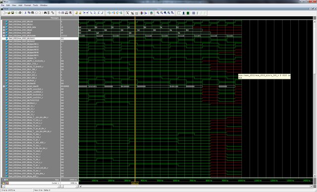
T0 seems to control when the next instruction is fetched, so it's important to have before I can get even the most basic parts of my 6502 core working :cry:

P.S. Sorry if this is posted to the wrong section. I'm working in Verilog, so I would have posted it in that section, but my question isn't actually related to verilog.

Any help is greatly appreciated. Thank you.
fachat
Posts: 1124
Joined: 05 Jul 2005
Location: near Heidelberg, Germany
Contact:

Post by fachat »

IIRC T0 is active in the last cycle of the previous opcode already. There may be a PLA (decoder) output to drive it low.

André
User avatar
BigEd
Posts: 11464
Joined: 11 Dec 2008
Location: England
Contact:

Post by BigEd »

Hi Xor
Welcome! It's worth taking a look at Peter Monta's FPGA netlist tools project. He takes the visual6502 data structures and makes a verilog netlist which is as high-level as he can get it - mostly logic gates, with some low-level stuff for the datapath busses.

The project contains the resultant verilog, so you don't even need to compile and run it. I believe the verilog contains many meaningful signal names from the visual6502 project too.

Peter's project produces a model which behaves as a 6502 - it doesn't in itself add any explanations as to how or why - so it should be complementary to your project

Cheers
Ed
Xor
Posts: 19
Joined: 10 Jan 2011

Post by Xor »

BigEd: That's a fantastic resource, thank you! It's still low level, which will still give me an opportunity to learn the architecture; the how and why. It will be a lot easier to read than the physical layout or transistor netlist, though :P

Yesterday I actually built a tool in JavaScript which takes the visual6502 netlist and allows me to enter a node and explore the transistors and connected nodes that drive it. So, for example, I could type in "clock1" and it'll search out, one depth at a time, what drives it.

It was handy, but I'm still new to mentally mapping nmos transistors into logic, so I didn't get very far.

Anyway, thank you again, that will be immensely helpful! :D
User avatar
BigEd
Posts: 11464
Joined: 11 Dec 2008
Location: England
Contact:

Post by BigEd »

Hi Xor
That tool sounds interesting - feel free to add it to visual6502 by joining in on github, or if you like, add an MIT-style license and send it to me and I'll see if I can merge it in.

The other day I found myself using the shift-click function on visual6502, which shows you all the nodes which are presently connected by pass gates. As you step through the simulation, you can see the busses connected and disconnected, and see which circuits are reading or writing. (I was working on this page about one of the unassigned opcodes.)

Cheers
Ed
Xor
Posts: 19
Joined: 10 Jan 2011

Post by Xor »

Hello BigEd:

I'll see what I can do. I'm neck deep in verilog right now trying to slowly decode what drives clock1. Thank you again for the link to that project!

There seems to be the occasional redundancy in the logic. For example node 17 and clock1 are the same thing, as far as I can tell. I guess that exists due to an electrical design decision in the actual 6502.

It'd be nice to write a tool that makes simple optimizations like that, so people working on projects like mine can start from a succinct netlist.
User avatar
Arlet
Posts: 2353
Joined: 16 Nov 2010
Location: Gouda, The Netherlands
Contact:

Post by Arlet »

Xor wrote:
It'd be nice to write a tool that makes simple optimizations like that, so people
working on projects like mine can start from a succinct netlist.
If you run the verilog through a synthesizer tool, it should report which signals are unused or duplicated.
Xor
Posts: 19
Joined: 10 Jan 2011

Post by Xor »

Well, thanks to the netlist->verilog project I've been able to make some progress. It's not much progress, but some is better than none at all.

So far I've distilled the logic into this:

Code: Select all

always @ (posedge cclk)
	pipe_T0 <= clock1;

always @ (posedge cp1_v)
begin
	clock2 <= pipe_T0 | notRdy0;
	clock1 <= ((n_1215 & _TWOCYCLE) | n_109) & ((!pipe_T0 & !notRdy0) | pipe_T0);
end
This is highly distilled; I manually deconstructed the logic from what the netlist->verilog project gives (which is rather low-level and crufted by analog processing elements). clock2 works as I expected; a delayed by one version of clock1, except when notRdy0 goes high.

clock1 is driven by various signals. Half of it drives clock1 high when it was low in the previous full-cycle. The other half is what drives it low (time to fetch a new instruction).

Again, it's not much, but I'm really happy to have made some progress. I verified my equations against visual6502 with a few random predictions done by hand. Seems to be correct. Now I need to continue my work and find out what drives 1215, #TWOCYCLE, and 109.

As a side note, notRdy0 is always 0 in the example program running on visual6502. I'm not sure why? Is it because the external memory is always "ready" in the visual6502 simulation? From what I can tell, notRdy0 tells the 6502 that RAM is busy (thus, not ready). So if I read this logic correctly, when clock1 goes low it will stay low as long as notRdy0 is high. In other words, the 6502 will sit and wait for RAM to stop goofing off. Neat! :D
Xor
Posts: 19
Joined: 10 Jan 2011

Post by Xor »

PHEW! It looks like I finally have enough logic built up to get something working. I just need to plug in a partial PLA and it should correctly fetch instructions and run the timing control:

Code: Select all

module 6502(clk, bi_data);

	input clk;
	inout [7:0] bi_data;

	reg [7:0] pd = 8'd0;
	reg clock1, clock2;


	// cclk domain
	reg pipeUNK11, pipeUNK23, pipeUNK35, pipeUNK40, pipeUNK41, pipe_T0;

	// cp1 domain
	reg n_24_v, n_653_v, n_666_v;

	wire cclk = clk;
	wire cp1 = !clk;


	/////////////////////////////////////////////////////////////////
	// Pre-Decoder
	wire fetch_v = pipeUNK11;
	wire clearIR_v = !fetch_v;

	wire [7:0] pd_clearIR = clearIR ? 8'd0 : pd;

	wire PD_xxxx10x0_v = !(pd_clearIR[0] | n_1083_v | pd_clearIR[2]);
	wire PD_1xx000x0_v = !(n_1605_v | pd_clearIR[0] | pd_clearIR[3] | pd_clearIR_v[4] | pd_clearIR[2]);
	wire PD_0xx0xx0x_v = !(pd_clearIR[7] | pd_clearIR[4] | pd_clearIR[1]);
	wire PD_xxx010x1_v = !(n_1083_v | pd_clearIR[4] | n_409_v | pd_clearIR[2]);
	wire PD_n_0xx0xx0x_v = !PD_0xx0xx0x_v;

	wire TWOCYCLE = (PD_n_0xx0xx0x_v & PD_xxxx10x0_v) | (PD_1xx000x0_v | PD_xxx010x1_v);
	/////////////////////////////////////////////////////////////////
	
	
	assign n_347_v = ~((op_T2_mem_zp_v|op_T3_mem_zp_idx_v|op_T3_mem_abs_v|op_T4_mem_abs_idx_v|op_T5_mem_ind_idx_v));
	assign n_790_v = ~((op_asl_rol_v|op_lsr_ror_dec_inc_v));
	assign n_368_v = ~((x_op_T3_plp_pla_v|op_T2_jmp_abs_v|op_T4_jmp_v|op_T5_rti_rts_v|xx_op_T5_jsr_v|op_T2_php_pha_v));


	wire n_1716_v = ~(op_T3_branch_v | n_653_v | !n_368_v);


	always @ (posedge cclk)
	begin
		pipeUNK11 <= !n_666_v;
		pipeUNK23 <= clock1;
		pipeUNK35 <= n_1716_v & pipeUNK23;
		pipeUNK40 <= !(n_790_v | n_347_v);
		pipeUNK41 <= n_24_v;

		pipe_T0 <= clock1;

		pd <= ~bi_data;
	end


	always @ (posedge cp1)
	begin
		n_24_v <= pipeUNK40;
		n_653_v <= !pipeUNK41;
		n_666_v <= pipeUNK23;
		
		// Timing Control
		clock1 <= (pipeUNK35 & !TWOCYCLE) | !pipe_T0;
		clock2 <= pipe_T0;
	end

endmodule

For now, I'm ignoring any nodes that are at fixed logic levels in the visual6502 demo. There's plenty of logic missing from the above that I assume has to do with instructions not exercised in the visual6502 demo; or corner cases (crossing page boundaries, for example). I'll eventually get back to those, but I'd like something partially working first. I have a separate, more complete file, which has TODO marks on all the incomplete signals.

At a quick glance, it looks like it handles 2 cycle instructions as a special case, with a quick 2 wide shift register to time those. The rest are handled by longer, conditional shift registers, I guess.
User avatar
BigEd
Posts: 11464
Joined: 11 Dec 2008
Location: England
Contact:

Post by BigEd »

Nice! I can see how this could grow into an annotated version which works exactly as the NMOS part, but well-structured and commented so it can be understood at a high level.

I particularly like the idea of growing it organically starting with instruction fetching.

Keep us updated!

Cheers
Ed

ps. yes, the visual6502 as presently released just has RDY held high, which is like single-cycle memory and is the normal case. The prerelease version on github can be stalled/unstalled for specific cycles by constructing a suitable URL.
Xor
Posts: 19
Joined: 10 Jan 2011

Post by Xor »

Thank you for the encouragement, BigEd.

After putting in the PLA, IR fetching logic, and fixing a few mistakes, I got it to work:

Image

For now, the test module manually feeds the correct data to the external databus. I'll need to add the logic for the address lines before it can run on its own.

Anyway, for the quick test, tcstate[0] and tcstate[1] were correct, which is what I've been working on.

With a little duct tape here, some bubble gum there, and a one paperclip I should have a fully working 6502 :P

By the way, whoever coded the "Trace These Too" feature on visual6502: many, many thanks! It's been so fantastically useful in debugging my code.
User avatar
Arlet
Posts: 2353
Joined: 16 Nov 2010
Location: Gouda, The Netherlands
Contact:

Post by Arlet »

Looks good. I'm also interested in the progress.

I did wonder about the dual clock. Right now you've inverted the clock, and are testing both edges. The simulator won't care, but have you tried running this through a synthesizer ? As far as I know, they usually aren't too happy with dual edge clocking.

An alternative may be to double the clock frequency, and run the phi1 stuff from even edges, and phi2 from odd edges using an extra enable signal.
Xor
Posts: 19
Joined: 10 Jan 2011

Post by Xor »

Arlet, yeah, the clocking is a little weird. I updated the clocking code to more closely model how the 6502 generates its clock. From what I remember in the documentation it pushes the edges of the two clocks away from each other; far enough that it satisfies setup and hold times.
When I synthesize I'll try to setup a PLL or two to correctly generate the dual-clock.

Thank you for commenting on that!


After a bit more muscle work I've extracted the necessary bits for running the AB, ADL, and PCL. So the chip can now manage its own PC and set its AB correctly. The other tcstates are also simulated correctly now.

Code: Select all

`timescale 1ns/1ns

module mos_6502(clk, ab, bi_data);

	input clk;
	inout [7:0] bi_data;
	output reg [15:0] ab = 16'h0000;


	reg [7:0] pd = 8'h00;
	reg [7:0] ir = 8'h00;
	reg [5:0] tcstate = 6'b111111;
	reg [7:0] pcl = 8'h00, pch = 8'h00;
	reg ADL_ABL = 1'b1;	// Load ADL into Address Bus Register Low
	reg I_PC = 1'b0;	// Increment Program Counter
	reg ADD_ADL = 1'b1, PCL_ADL = 1'b0, S_ADL = 1'b0, DL_ADL = 1'b0;	// Flags that select the source for Address Data Low
	reg [7:0] DL = 8'h00, S = 8'h00, ADD = 8'h00;
	wire [7:0] ADL = S_ADL ? S : (PCL_ADL ? pcl : (DL_ADL ? DL : (ADD_ADL ? ADD : 8'h00)));

	// Status Register
	reg p0 = 1'b0, p1 = 1'b1, p2 = 1'b1, p3 = 1'b0, p4 = 1'b1, p6 = 1'b0, p7 = 1'b0;

	wire clock1 = tcstate[0], clock2 = tcstate[1];


	// cclk domain
	reg pipeUNK11 = 1'b0, pipeUNK23 = 1'b0, pipeUNK35 = 1'b0, pipeUNK40 = 1'b0, pipeUNK41 = 1'b1, pipe_T0 = 1'b0, pipeBRtaken_v = 1'b0;

	// cp1 domain
	reg n_24_v = 1'b1, n_653_v = 1'b0, n_666_v = 1'b0;

	reg cclk, cp1, shifted_clk;
	always #100 shifted_clk = clk;

	always @ (posedge shifted_clk) cclk <= 1'b1;
	always @ (negedge clk) cclk <= 1'b0;

	always @ (negedge shifted_clk) cp1 <= 1'b1;
	always @ (posedge clk) cp1 <= 1'b0;


	/////////////////////////////////////////////////////////////////
	// Pre-Decoder
	wire fetch_v = pipeUNK11;
	wire clearIR = !fetch_v;

	wire [7:0] pd_clearIR = clearIR ? 8'd0 : pd;

	wire PD_xxxx10x0_v = !(pd_clearIR[0] | !pd_clearIR[3] | pd_clearIR[2]);
	wire PD_1xx000x0_v = !(!pd_clearIR[7] | pd_clearIR[0] | pd_clearIR[3] | pd_clearIR[4] | pd_clearIR[2]);
	wire PD_0xx0xx0x_v = !(pd_clearIR[7] | pd_clearIR[4] | pd_clearIR[1]);
	wire PD_xxx010x1_v = !(!pd_clearIR[3] | pd_clearIR[4] | !pd_clearIR[0] | pd_clearIR[2]);
	wire PD_n_0xx0xx0x_v = !PD_0xx0xx0x_v;

	wire TWOCYCLE = (PD_n_0xx0xx0x_v & PD_xxxx10x0_v) | (PD_1xx000x0_v | PD_xxx010x1_v);
	/////////////////////////////////////////////////////////////////
	

	// PLA
	// TODO: This should be a module that takes the appropriate inputs and
	// gives a large 130 bit output. We can then write an include that
	// assigns named wires to the bit array.
	`include "pla_decode.v"
	
	
	assign n_256_v = ~((op_T5_ind_x_v|op_T0_brk_rti_v|op_T0_jmp_v|op_T5_rts_v|op_T4_v|op_T5_rti_v|op_T3_v));
	assign n_347_v = ~((op_T2_mem_zp_v|op_T3_mem_zp_idx_v|op_T3_mem_abs_v|op_T4_mem_abs_idx_v|op_T5_mem_ind_idx_v));
	assign n_790_v = ~((op_asl_rol_v|op_lsr_ror_dec_inc_v));
	assign n_368_v = ~((x_op_T3_plp_pla_v|op_T2_jmp_abs_v|op_T4_jmp_v|op_T5_rti_rts_v|xx_op_T5_jsr_v|op_T2_php_pha_v));
	

	wire n_1716_v = ~(op_T3_branch_v | n_653_v | !n_368_v);
	wire n_1286_v = ~(op_brk_rti_v | x_op_jmp_v | op_jsr_v | clock1);
	wire n_1211_v = ~(op_T5_jsr_v | op_T2_branch_v | n_1286_v | !n_666_v | op_T2_abs_access_v);
	wire n_182_v = clock1 & !op_T5_rts_v & n_1211_v;
	wire n_1619_v = !(op_T2_branch_v | n_182_v);
	wire n_620_v = (_op_branch_bit7_v | _op_branch_bit6_v | !p1) & (!p0 | !_op_branch_bit6_v | _op_branch_bit7_v);
	wire BRtaken_v = (ir[5] | !(_op_branch_bit7_v | _op_branch_bit6_v | !p1) ) & (!ir[5] | n_620_v);


	always @ (posedge cclk)
	begin
		pipeUNK11 <= !n_666_v;
		pipeUNK23 <= clock1;
		pipeUNK35 <= n_1716_v & clock1;
		pipeUNK40 <= !(n_790_v | n_347_v);
		pipeUNK41 <= n_24_v;

		pipe_T0 <= clock1;
		pipeBRtaken_v <= !(n_1619_v | (BRtaken_v & op_T2_branch_v));

		pd <= bi_data;

		// Bus Control Signals
		ADL_ABL <= !n_653_v & n_24_v;
		ADD_ADL <= !n_256_v;
		PCL_ADL <= op_T5_jsr_v | op_T2_branch_v | op_T2_abs_access_v | ( !( op_brk_rti_v | x_op_jmp_v | op_jsr_v ) & !clock1 ) | !n_666_v;
		S_ADL <= op_T2_stack_v | op_T0_jsr_v;
		DL_ADL <= op_T2_ind_v | op_T2_zp_zp_idx_v;
	end


	always @ (posedge cp1)
	begin
		n_24_v <= !pipeUNK40;
		n_653_v <= !pipeUNK41;
		n_666_v <= pipeUNK23;

		if(ADL_ABL)
			ab[7:0] <= ADL;

		// Increment PC?
		I_PC <= pipeBRtaken_v | PD_xxxx10x0_v;

		if(!I_PC)
			{pch, pcl} <= {pch, pcl} + 16'd1;

		if(fetch_v)
			ir <= pd_clearIR;
		
		// Timing Control
		tcstate[0] <= (pipeUNK35 & !TWOCYCLE) | !pipe_T0;
		tcstate[1] <= pipe_T0;
		tcstate[2] <= tcstate[1];

		if(!tcstate[0])
			tcstate[5:3] <= 3'b111;
		else
			tcstate[5:3] <= tcstate[4:2];
	end

endmodule

My short-term goal is to get the visual6502 example program working. To that end I'll start the arduous task of bashing my now swollen head into the keyboard until verilog code eventually falls out of it.
Or just get DL, AC, and the associated control signals working ...
User avatar
Arlet
Posts: 2353
Joined: 16 Nov 2010
Location: Gouda, The Netherlands
Contact:

Post by Arlet »

I don't know how often this is possible, but when you're all done with the first implementation, it may be good to try to identify latches that are clocked by two phases, and substitute them with a single edge flip flop.

In my verilog 6502 model, I started from the other end. I decided on a single clock from the beginning, and didn't worry too much about 100% authentic behavior at every bus cycle. I just tried to get as close as possible.

It would be interesting to see how close these two approaches can get, and how they differ in area, speed, and accuracy.
Xor
Posts: 19
Joined: 10 Jan 2011

Post by Xor »

Arlet: To be honest, I would much prefer to have done a single clock implementation from the beginning :P My job affords me the luxury of working with single clock systems all the time, with only the occasional need to cross clock domains (which I despise doing and debugging). But building this accurate implementation of the 6502 is a great learning experience for me, if for nothing else than working with dual-clocks.

As a side note, I believe the code I've written thus far is ever so slightly incorrect. It's registered, whereas the 6502 uses latches. So, for example:

Code: Select all

always @ (posedge cp1)
begin
	n_24_v <= !pipeUNK40;
end
Should really be:

Code: Select all

always @ *
if (cp1)
begin
	n_24_v <= !pipeUNK40;
end
which should correctly simulate a latch. I've always worked with registers, so I'm not even sure if the above would synthesize on the FPGAs I work with.

So far I've just worked around the differences but I may go back and update the code to be more accurate.
Post Reply