I see a switch in the schematic but it is not tied to Vcc anywhere.
Right. VCC and GND go to the supply pins of the inverter IC (as Yuri said), but in this circuit they don't attach to the switch.
How the circuit works:
It's maybe best to start by pointing out that the two inverters are connected to act as a memory (aka, a flip-flop). If the output happens to be high then it will stay high, and if it happens to be low then it will stay low. These two possible circumstances are shown in the diagram below. (As you can see, I've stripped away the other components.)
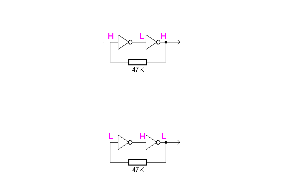
- detail a.png (2.59 KiB) Viewed 5006 times
When the other components are added we can see that the capacitor will slowly (ie; about 50 ms, because of the large resistance) charge or discharge until
the capacitor is in the opposite state compared to the input of the first inverter.

And the circuit will remain in this condition while it's waiting for the button to be pushed. Once again the diagram shows the two stable circumstances which are possible.
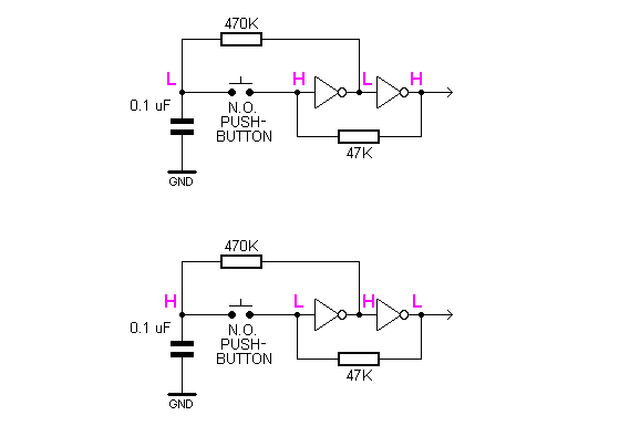
- detail b.png (3.94 KiB) Viewed 5006 times
When the button is pushed, the high or low state of the capacitor gets applied to the input of the first inverter, causing that input to go high if it was low, or go low if it was high. (The cap momentarily overpowers the influence of the 47K resistor; then the flip-flop changes state and the resistor no longer needs to be overpowered.)
During the time the button remains pressed, the capacitor and the input of the first inverter will be in agreement rather than opposition. The cap won't appreciably charge or discharge because during this time it is influenced primarily by the small, 47K resistor. But when the button is
released, then the large, 470K resistor will
slowly cause the capacitor to update until it's once again in opposition, ready for the following button-push. And this slowness is what gives the circuit its immunity to contact bounce.
BTW, the circuit as shown is intended for use with inverters (or inverting gates such as NAND or NOR) from one of the CMOS families, for example the 74HC family, 74AHC, or, with caveats, even the old 4000 CMOS family. Inverters/gates which have Schmitt-trigger inputs are also acceptable (or maybe even slightly preferred, as the Schmitt-trigger inputs will avoid the small, theoretical risk that the circuit might falter on a tiny minority of the button-pushes.)
As for logic families such as 74HC
T and 74LS, these are not very good choices -- it's doubtful whether they can be coaxed to work. I can't say for sure it's impossible, but I
am sure it would require some expert tinkering to modify the circuit.
-- Jeff


