I know that WinCUPL is free software so I shouldn't complain, but you'd think that they'd fix such an obvious and important bug?
GAL Address Decoder
- BigDumbDinosaur
- Posts: 9425
- Joined: 28 May 2009
- Location: Midwestern USA (JB Pritzker’s dystopia)
- Contact:
Re: GAL Address Decoder
banedon wrote:
Thanks for advising as I may have wasted a lot more time on using FIELDs.
I know that WinCUPL is free software so I shouldn't complain, but you'd think that they'd fix such an obvious and important bug?
Quote:
Unless perhaps it's device specific?
Quote:
[EDIT] I've emailed Atmel to see what they say. Not sure it'll do any good, but they might be able to shed a little light.
x86? We ain't got no x86. We don't NEED no stinking x86!
Re: GAL Address Decoder
Looks like there's an odd feature that variables which end in digits are used as column indices. See
http://www.edaboard.co.uk/help-with-atf ... 00493.html
which says you either need to align your table data very carefully in the right columns, or use variable names which don't end in digits.
http://www.edaboard.co.uk/help-with-atf ... 00493.html
which says you either need to align your table data very carefully in the right columns, or use variable names which don't end in digits.
- BigDumbDinosaur
- Posts: 9425
- Joined: 28 May 2009
- Location: Midwestern USA (JB Pritzker’s dystopia)
- Contact:
Re: GAL Address Decoder
BigEd wrote:
Looks like there's an odd feature that variables which end in digits are used as column indices. See
http://www.edaboard.co.uk/help-with-atf ... 00493.html
which says you either need to align your table data very carefully in the right columns, or use variable names which don't end in digits.
http://www.edaboard.co.uk/help-with-atf ... 00493.html
which says you either need to align your table data very carefully in the right columns, or use variable names which don't end in digits.
Another one of WinCUPL's obscure bugs has to do with case-sensitivity. Officially, CUPL as developed by Logical Devices Inc. is case-sensitive for variable names. Given that, one would think that via_sel and VIA_SEL would be seen as two unrelated variables. That's not the case with the simulator function associated with WinCUPL, as I discovered early on. An example program that I wrote would compile but not simulate, with the simulator reporting errors that made no sense. Here's the reply I got from Atmel:
- The WinSim issue seems to be caused by the use of “wd” and “WD” in the CUPL design file. I tried changing “WD” to “WD_t” and that fixed the WinSim problem.
Hope this will help you solve the problem. Please feel free to contact us at pld@atmel.com if you have any Atmel PLD related inquiries.
Best regards,
Alan Wong
CSP Applications Manager / Atmel Corporation
Tel: (+1) (408) 436-4156 / Fax: (+1) (408) 487-2538
Alan.Wong@atmel.com / http://www.atmel.com
x86? We ain't got no x86. We don't NEED no stinking x86!
Re: GAL Address Decoder
Here's the results of my decoder under simulation - all looks fine:
The data it ran with:
That's an excellent idea, Peter. Many thanks
. I'll almost certainly implement it.
I'll also have a think on your other idea.
Code: Select all
Name AddressDecoder;
PartNo Lattice22V10B;
Date 02/04/15;
Revision 01;
Designer shalewyn.com;
Company shalewyn.com;
Assembly XXXXX;
Location XXXXX;
Device g22v10;
ORDER: PHI2, R_W, A15, A14, A13, A12, A6, A5, A4, sb0, sb1, !RD, !WR, !IO, !BASERAM, !SWAPBANK0, !SWAPBANK1, !SWAPBANK2, !SWAPBANK3, !ROM;
VECTORS:
1 1 0 0 0 0 1 1 1 0 1 * * * * * * * * *
1 0 0 1 1 0 1 1 1 1 1 * * * * * * * * *
0 0 1 0 0 1 1 0 1 0 1 * * * * * * * * *
1 1 0 0 1 1 0 0 1 1 0 * * * * * * * * *
1 0 0 1 0 1 1 0 1 0 0 * * * * * * * * *
1 1 1 0 1 1 0 1 1 0 0 * * * * * * * * *
0 1 0 0 0 0 0 0 1 1 1 * * * * * * * * *
1 1 1 1 1 1 1 0 1 1 0 * * * * * * * * *cbscpe wrote:
...As for bankswitching, sometimes you want to copy data from one bank to the other, therefore I would introduce 4 bankswitching signals, one set of 2 signals that control the bank you read from and 2 signals that control the bank you write to
without creating select signals for the RAM you have plenty of free pins on your GAL...
Code: Select all
R15 = !A15 & !A14 & A13 & sb0r & RW
# !A15 & A14 & sb0r & RW
# !A15 & !A14 & A13 & sb0w & !RW
# !A15 & A14 & sb0w & !RW
R15 = !A15 & !A14 & A13 & sb1r & RW
# !A15 & A14 & sb1r & RW
# !A15 & !A14 & A13 & sb1w & !RW
# !A15 & A14 & sb1w & !RW
I'll also have a think on your other idea.
Re: GAL Address Decoder
Ok here we are with the dual read bank, write bank implemented (Many thanks to Peter).
I get an odd error with this, though, when trying to simulate it. It seems to generate a parse error in the .SO file when compiled from WinCUPL. If I then go into the Simulator and compile it I end up with what I expected.
Here's the code and the data I ran it with. Can anyone else reproduce the error?
There .SI file:
And my eventual results after recompiling from within the Simulator:
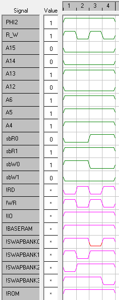
Confirmed as working (so far) in a GAL
[EDIT] I've just removed A5-A7 (pins 7-9) as they are not used. Frees up 3 pins for future use.
I get an odd error with this, though, when trying to simulate it. It seems to generate a parse error in the .SO file when compiled from WinCUPL. If I then go into the Simulator and compile it I end up with what I expected.
Here's the code and the data I ran it with. Can anyone else reproduce the error?
Code: Select all
Name AddressDecoder;
Partno Lattice22V10B;
Date 02/04/15;
Revision 01;
Designer shalewyn.com;
Company shalewyn.com;
Assembly XXXXX;
Location XXXXX;
Device g22v10;
/*
* Lattice GAL 22V10B pinout, DIP, top view
*
* I/CLK.[ 1 24 ].VCC
* I.[ 2 23 ].I/O/Q
* I.[ 3 22 ].I/O/Q
* I.[ 4 21 ].I/O/Q
* I.[ 5 20 ].I/O/Q
* I.[ 6 19 ].I/O/Q
* I.[ 7 18 ].I/O/Q
* I.[ 8 17 ].I/O/Q
* I.[ 9 16 ].I/O/Q
* I.[ 10 15 ].I/O/Q
* I.[ 11 14 ].I/O/Q
* GND.[ 12 13 ].I
*
*
*
* $1000-$1FFF BaseRAM %0000 0000 0000 0000 - %0001 1111 1111 1111
* $2000-$7FFF SwapRAM %0010 0000 0000 0000 - %0111 1111 1111 1111
* $8010-$801F VIA #1 (I/O) %1000 0000 0001 0000 - %1000 0000 0000 1111
* $8020-$802F VIA #2 (I/O) %1000 0000 0010 0000 - %1000 0000 0001 1111
* $8040-$804F ACIA (I/O) %1000 0000 0100 0000 - %1000 0000 0010 1111
* $9000-$FFFF ROM %1001 0000 0000 0000 - %1111 1111 1111 1111
*
*
*
* Inputs
*/
/* Inputs */
PIN 1 = PHI2;
PIN 2 = R_W;
PIN [3..6] = [A15..12];
PIN [7..9] = [A6..4];
PIN 10 = sbR0;
PIN 11 = sbR1;
PIN 13 = sbW0;
PIN 14 = sbW1;
/* Outputs */
PIN 15 = !RD;
PIN 16 = !WR;
PIN 17 = !IO;
PIN 18 = !BASERAM;
PIN 19 = !SWAPBANK0;
PIN 20 = !SWAPBANK1;
PIN 21 = !SWAPBANK2;
PIN 22 = !SWAPBANK3;
PIN 23 = !ROM;
/* Main */
RD = PHI2 & R_W;
WR = PHI2 & !R_W;
BASERAM = !A15 & !A14 & !A13;
SWAPBANK0 = !A15 & !A14 & A13 & !A12 & !sbR0 & !sbR1 & WR
# !A15 & !A14 & A13 & A12 & !sbR0 & !sbR1 & WR
# !A15 & A14 & !A13 & !A12 & !sbR0 & !sbR1 & WR
# !A15 & A14 & !A13 & A12 & !sbR0 & !sbR1 & WR
# !A15 & A14 & A13 & !A12 & !sbR0 & !sbR1 & WR
# !A15 & A14 & A13 & A12 & !sbR0 & !sbR1 & WR
# !A15 & !A14 & A13 & !A12 & !sbW0 & !sbW1 & !WR
# !A15 & !A14 & A13 & A12 & !sbW0 & !sbW1 & !WR
# !A15 & A14 & !A13 & !A12 & !sbW0 & !sbW1 & !WR
# !A15 & A14 & !A13 & A12 & !sbW0 & !sbW1 & !WR
# !A15 & A14 & A13 & !A12 & !sbW0 & !sbW1 & !WR
# !A15 & A14 & A13 & A12 & !sbW0 & !sbW1 & !WR;
SWAPBANK1 = !A15 & !A14 & A13 & !A12 & !sbR0 & sbR1 & WR
# !A15 & !A14 & A13 & A12 & !sbR0 & sbR1 & WR
# !A15 & A14 & !A13 & !A12 & !sbR0 & sbR1 & WR
# !A15 & A14 & !A13 & A12 & !sbR0 & sbR1 & WR
# !A15 & A14 & A13 & !A12 & !sbR0 & sbR1 & WR
# !A15 & A14 & A13 & A12 & !sbR0 & sbR1 & WR
# !A15 & !A14 & A13 & !A12 & !sbW0 & sbW1 & !WR
# !A15 & !A14 & A13 & A12 & !sbW0 & sbW1 & !WR
# !A15 & A14 & !A13 & !A12 & !sbW0 & sbW1 & !WR
# !A15 & A14 & !A13 & A12 & !sbW0 & sbW1 & !WR
# !A15 & A14 & A13 & !A12 & !sbW0 & sbW1 & !WR
# !A15 & A14 & A13 & A12 & !sbW0 & sbW1 & !WR;
SWAPBANK2 = !A15 & !A14 & A13 & !A12 & sbR0 & !sbR1 & WR
# !A15 & !A14 & A13 & A12 & sbR0 & !sbR1 & WR
# !A15 & A14 & !A13 & !A12 & sbR0 & !sbR1 & WR
# !A15 & A14 & !A13 & A12 & sbR0 & !sbR1 & WR
# !A15 & A14 & A13 & !A12 & sbR0 & !sbR1 & WR
# !A15 & A14 & A13 & A12 & sbR0 & !sbR1 & WR
# !A15 & !A14 & A13 & !A12 & sbW0 & !sbW1 & !WR
# !A15 & !A14 & A13 & A12 & sbW0 & !sbW1 & !WR
# !A15 & A14 & !A13 & !A12 & sbW0 & !sbW1 & !WR
# !A15 & A14 & !A13 & A12 & sbW0 & !sbW1 & !WR
# !A15 & A14 & A13 & !A12 & sbW0 & !sbW1 & !WR
# !A15 & A14 & A13 & A12 & sbW0 & !sbW1 & !WR;
SWAPBANK3 = !A15 & !A14 & A13 & !A12 & sbR0 & sbR1 & WR
# !A15 & !A14 & A13 & A12 & sbR0 & sbR1 & WR
# !A15 & A14 & !A13 & !A12 & sbR0 & sbR1 & WR
# !A15 & A14 & !A13 & A12 & sbR0 & sbR1 & WR
# !A15 & A14 & A13 & !A12 & sbR0 & sbR1 & WR
# !A15 & A14 & A13 & A12 & sbR0 & sbR1 & WR
# !A15 & !A14 & A13 & !A12 & sbW0 & sbW1 & !WR
# !A15 & !A14 & A13 & A12 & sbW0 & sbW1 & !WR
# !A15 & A14 & !A13 & !A12 & sbW0 & sbW1 & !WR
# !A15 & A14 & !A13 & A12 & sbW0 & sbW1 & !WR
# !A15 & A14 & A13 & !A12 & sbW0 & sbW1 & !WR
# !A15 & A14 & A13 & A12 & sbW0 & sbW1 & !WR;
IO = A15 & !A14 & !A13 & !A12 & !A5 & !A4;
ROM = A15 & !A14 & !A13 & A12
# A15 & !A14 & A13 & !A12
# A15 & !A14 & A13 & A12
# A15 & A14 & !A13 & !A12
# A15 & A14 & !A13 & A12
# A15 & A14 & A13 & !A12
# A15 & A14 & A13 & A12;Code: Select all
Name AddressDecoder;
PartNo Lattice22V10B;
Date 02/04/15;
Revision 01;
Designer shalewyn.com;
Company shalewyn.com;
Assembly XXXXX;
Location XXXXX;
Device g22v10;
ORDER: PHI2, R_W, A15, A14, A13, A12, A6, A5, A4, sbR0, sbR1, sbW0, sbW1, !RD, !WR, !IO, !BASERAM, !SWAPBANK0, !SWAPBANK1, !SWAPBANK2, !SWAPBANK3, !ROM;
VECTORS:
1 1 0 0 1 0 1 1 1 0 1 1 0 * * * * * * * * *
1 0 0 0 1 0 1 1 1 0 1 1 0 * * * * * * * * *
1 1 0 0 1 0 1 1 1 1 1 0 0 * * * * * * * * *
1 0 0 0 1 0 1 1 1 1 1 0 0 * * * * * * * * *Confirmed as working (so far) in a GAL
[EDIT] I've just removed A5-A7 (pins 7-9) as they are not used. Frees up 3 pins for future use.
- BitWise
- In Memoriam
- Posts: 996
- Joined: 02 Mar 2004
- Location: Berkshire, UK
- Contact:
Re: GAL Address Decoder
BigDumbDinosaur wrote:
banedon wrote:
Thanks for advising as I may have wasted a lot more time on using FIELDs.
I know that WinCUPL is free software so I shouldn't complain, but you'd think that they'd fix such an obvious and important bug?
Quote:
Unless perhaps it's device specific?
Andrew Jacobs
6502 & PIC Stuff - http://www.obelisk.me.uk/
Cross-Platform 6502/65C02/65816 Macro Assembler - http://www.obelisk.me.uk/dev65/
Open Source Projects - https://github.com/andrew-jacobs
6502 & PIC Stuff - http://www.obelisk.me.uk/
Cross-Platform 6502/65C02/65816 Macro Assembler - http://www.obelisk.me.uk/dev65/
Open Source Projects - https://github.com/andrew-jacobs
Re: GAL Address Decoder
I know I'm kind of late, but I took up the problem with the FIELD and TABLE command and have it worked out I think.
Here's the source:
I noticed a few things on your original post. The Selects field had 6 bits vs. 5, so I corrected that.
It also appears that it does not matter if I define Selects as [s4..0] or [s0..4], WinCUPL formats it as [s4..0].
The manual also said the default value is HEX so I removed the 'h' prefixes. The example in the manual also had a full
16-bit hex address even thought the AddressBus only had A15..A12 defined, so it must strip off any extra bits. That is why I used the
full 16-bit address in the table.
Here is the output from the Simulator (click to enlarge):
Vector 1 = $0000
Vector 2 = $2000
Vector 3 = $8000
Vector 4 = $8010
Vector 5 = $8020
Vector 6 = $8040
Vector 7 = $9000
Vector 8 = $FFFF
It appears correct in the simulation, I have not tried it on actual silicon.
Daryl
Here's the source:
Code: Select all
Name AddressDecoder;
Partno Lattice22V10B;
Date 02/04/15;
Revision 01;
Designer shalewyn.com;
Company shalewyn.com;
Assembly 1;
Location 1;
Device g22v10;
/*
* Lattice GAL 22V10B pinout, DIP, top view
*
* I/CLK.[ 1 24 ].VCC
* I.[ 2 23 ].I/O/Q
* I.[ 3 22 ].I/O/Q
* I.[ 4 21 ].I/O/Q
* I.[ 5 20 ].I/O/Q
* I.[ 6 19 ].I/O/Q
* I.[ 7 18 ].I/O/Q
* I.[ 8 17 ].I/O/Q
* I.[ 9 16 ].I/O/Q
* I.[ 10 15 ].I/O/Q
* I.[ 11 14 ].I/O/Q
* GND.[ 12 13 ].I
*
*
*
* $1000-$1FFF - %0001 0000 0000 0000 - %0001 1111 1111 1111
* $2000-$2FFF - %0010 0000 0000 0000 - %0111 1111 1111 1111
* $8000-$800F - %1000 0000 0000 0000 - %1000 0000 0000 1111
* $8010-$801F - %1000 0000 0001 0000 - %1000 0000 0001 1111
* $8020-$802F - %1000 0000 0010 0000 - %1000 0000 0010 1111
* $8040-$804F - %1000 0000 0100 0000 - %1000 0000 0100 1111
* $9000-$FFFF - %1001 0000 0000 0000 - %1111 1111 1111 1111
*
*
* !Pin 18 - non-swap RAM $0000-$1FFF
* !Pin 19 - Swap bank 0 or bank 1 - $2000-$7FFF
* !Pin 20 - /VIA 1 - $8000-$800F
* !Pin 21 - /VIA 2 - $8010-$801F
* !Pin 22 - /ROM - $9000-$FFFF
*
*
* Inputs
*/
Pin 1 = phi2;
Pin 2 = cpuRW;
Pin [3..11] = [A15..7];
Pin [13..15] = [A6..4];
Pin 16 = Swapbit;
/*
* Outputs
*/
/*
* Pin 18 = !selBaseRAM;
* Pin 19 = !selSwapRAMbank;
* Pin 20 = !selVIA1;
* Pin 21 = !selVIA2;
* Pin 22 = !selROM;
* Pin 23 = !WE out;
*/
Pin [18..22] = [s0..4];
/*
* Main
*/
FIELD AddressBus = [A15..4];
FIELD Selects = [s4..0];
TABLE AddressBus => Selects {
[0000..01FF] => 'b'00001; /* S0 - Non-swap RAM */
[2000..7FFF] => 'b'00010; /* S1 - Swap RAM */
[8000..800F] => 'b'00100; /* S2 - VIA 1 */
[8010..801F] => 'b'01000; /* S3 - VIA 2 */
[8020..8FFF] => 'b'00000; /* none */
[9000..FFFF] => 'b'10000; /* S4 - ROM */
}
It also appears that it does not matter if I define Selects as [s4..0] or [s0..4], WinCUPL formats it as [s4..0].
The manual also said the default value is HEX so I removed the 'h' prefixes. The example in the manual also had a full
16-bit hex address even thought the AddressBus only had A15..A12 defined, so it must strip off any extra bits. That is why I used the
full 16-bit address in the table.
Here is the output from the Simulator (click to enlarge):
Vector 1 = $0000
Vector 2 = $2000
Vector 3 = $8000
Vector 4 = $8010
Vector 5 = $8020
Vector 6 = $8040
Vector 7 = $9000
Vector 8 = $FFFF
It appears correct in the simulation, I have not tried it on actual silicon.
Daryl
Please visit my website -> https://sbc.rictor.org/
Re: GAL Address Decoder
Hi 8bit
Nice work. So it's just badly explained in the documentation or have I just misunderstood it? Either way, how would you go about adding the swap bank selects? They're comprised of 2 read bits (sbR0, sbR1) and 2 write bits (sbW0, sbW1). These can give a pattern of 00, 01, 10, 11 to gives 4 possible banks that can be read from and written to, but reading and writing can be to separate banks.
I was looking at the APPEND command for this, but I think that just adds an OR and then your code afterwards.
I.e. APPEND s0 = sbR0 & !sbR1; would simply add # (sbR0 & !sbR1); from what I understand. Where-as I would need to add something into the table itself...
Time for some experimentation!
Last edited by banedon on Sat Apr 04, 2015 5:34 pm, edited 1 time in total.
Re: GAL Address Decoder
Ok, the following seems to work. I've added in the bank control selects with appropriate inputs and restrictd the ability to write to a device until phi2 goes HI.
Test results
Code: Select all
Name AddressDecoder;
Partno Lattice22V10B;
Date 02/04/15;
Revision 01;
Designer shalewyn.com;
Company shalewyn.com;
Assembly 1;
Location 1;
Device g22v10;
/*
* Lattice GAL 22V10B pinout, DIP, top view
*
* I/CLK.[ 1 24 ].VCC
* I.[ 2 23 ].I/O/Q
* I.[ 3 22 ].I/O/Q
* I.[ 4 21 ].I/O/Q
* I.[ 5 20 ].I/O/Q
* I.[ 6 19 ].I/O/Q
* I.[ 7 18 ].I/O/Q
* I.[ 8 17 ].I/O/Q
* I.[ 9 16 ].I/O/Q
* I.[ 10 15 ].I/O/Q
* I.[ 11 14 ].I/O/Q
* GND.[ 12 13 ].I
*
*
*
* $0000-$1FFF : %0000 0000 0000 0000 - %0001 1111 1111 1111 : Base RAM area
* $2000-$7FFF : %0010 0000 0000 0000 - %0111 1111 1111 1111 : Swap RAM area
* $8000-$8FFF : %1000 0000 0000 0000 - %1000 1111 1111 1111 : I/O area (VIAs, ACIAs, etc.)
* $9000-$FFFF : %1001 0000 0000 0000 - %1111 1111 1111 1111 : ROM
*
*
*
* Inputs
*/
Pin 1 = phi2;
Pin 2 = cpuRW;
Pin [3..6] = [A15..12];
Pin 13 = SbR0;
Pin 14 = SbR1;
Pin 15 = SbW0;
Pin 16 = SbW1;
/*
* Outputs
*/
/* s0 - NonSWAP RAM
* s1 - Swap RAM bank 0
* s2 - Swap RAM bank 1
* s3 - Swap RAM bank 2
* s4 - Swap RAM bank 3
* s5 - I/O (VIAs, ACIAs, etc.)
* s6 - ROM */
Pin [17..23] = ![s0..6];
/*
* Main
*/
FIELD AddressBus = [A15..12];
FIELD Selects = [s6..0];
/* Note that each device which can be written to has 2 entries - one for reading and
* one for writing. This is because writing should only ever happen when phi2 is HI
* so we need one rule which allows read if cpuRW is HI and one rule which only
* allows writes when cpuRW is LOW and phi2 is HI. */
TABLE AddressBus => Selects {
[0000..1FFF] => 'b'0000001 & cpuRW; /* S0 - Non-swap RAM read */
[0000..1FFF] => 'b'0000001 & !cpuRW & phi2; /* S0 - Non-swap RAM write */
[2000..7FFF] => 'b'0000010 & !SbR0 & !SbR1 & cpuRW; /* S1 - Swap RAM read bank 0*/
[2000..7FFF] => 'b'0000100 & !SbR0 & SbR1 & cpuRW; /* S2 - Swap RAM read bank 1 */
[2000..7FFF] => 'b'0001000 & SbR0 & !SbR1 & cpuRW; /* S3 - Swap RAM read bank 2 */
[2000..7FFF] => 'b'0010000 & SbR0 & SbR1 & cpuRW; /* S4 - Swap RAM read bank 3 */
[2000..7FFF] => 'b'0000010 & !SbW0 & !SbW1 & !cpuRW & phi2;/* S1 - Swap RAM write bank 0 */
[2000..7FFF] => 'b'0000100 & !SbW0 & SbW1 & !cpuRW & phi2; /* S2 - Swap RAM write bank 1 */
[2000..7FFF] => 'b'0001000 & SbW0 & !SbW1 & !cpuRW & phi2; /* S3 - Swap RAM write bank 2 */
[2000..7FFF] => 'b'0010000 & SbW0 & SbW1 & !cpuRW & phi2; /* S4 - Swap RAM write bank 3 */
[8000..8FFF] => 'b'0100000 & cpuRW; /* S5 - IO read */
[8000..8FFF] => 'b'0100000 & !cpuRW & phi2; /* S5 - IO write*/
[9000..FFFF] => 'b'1000000; /* S6 - ROM */
}Code: Select all
Name AddressDecoder;
PartNo Lattice22V10B;
Date 02/04/15;
Revision 01;
Designer shalewyn.com;
Company shalewyn.com;
Assembly 1;
Location 1;
Device g22v10;
ORDER: phi2, cpuRW, A15..A12, SbR0, SbR1, SbW0, SbW1, !s0, !s1, !s2, !s3, !s4, !s5, !s6;
VECTORS:
/* each test comprises of a set of read and a set of writes.
* 1st test is for PHI2 being HI and the 2nd for PHI being LOW */
/* Base RAM test 2xRead, 2xW1rite */
11 '1' 0110*******
01 '1' 0110*******
10 '1' 0110*******
00 '1' 0110*******
/* Swap RAM bank 1 read, bank 2 write tests 2xRead, 2xWrite */
11 '2' 0110*******
01 '2' 0110*******
10 '2' 0110*******
00 '2' 0110*******
/* Swap RAM bank 3 read, bank 0 write tests 2xRead, 2xWrite */
11 '2' 1100*******
01 '2' 1100*******
10 '2' 1100*******
00 '2' 1100*******
/* I/O test 2xRead, 2xW1rite */
11 '8' 1100*******
01 '8' 1100*******
10 '8' 1100*******
00 '8' 1100*******
/* ROM test 2xRead */
11 'F' 1100*******
01 'F' 1100*******Re: GAL Address Decoder
And finally here's the 1Mbit RAM IC version. This one doesn't use 4 different modules, but utilises a 1Mbit (128KB) RAM. It splits the IC into quarters, maps banks 0-3 to each quarter by controlling A15 and A16 address pins.
Base RAM sits in the first quarter (bank 0).
Memory map now looks something like this: Total RAM space is:
24KB x 4 banks = 96KB + 8KB base RAM = 104KB Total RAM
Additionally, you have 4KB of I/O address space and 28KB of ROM space for the OS.
Total addressable space (by cheating)? 136KB. Not too shoddy.
Please see attached for the .PLD and .SI files (I had to rename them as TXT so I cold upload them to the forum):
[EDIT] Now changed to be compatible with the 65C816 (thanks BigD
)
My next step is to drop this into a 4Mbit SRAM and also find a way of possibly using the slack 8KB lost in each bank area except bank 0 (i.e. +$0 to +$1FFF).
Base RAM sits in the first quarter (bank 0).
Memory map now looks something like this: Total RAM space is:
24KB x 4 banks = 96KB + 8KB base RAM = 104KB Total RAM
Additionally, you have 4KB of I/O address space and 28KB of ROM space for the OS.
Total addressable space (by cheating)? 136KB. Not too shoddy.
Please see attached for the .PLD and .SI files (I had to rename them as TXT so I cold upload them to the forum):
[EDIT] Now changed to be compatible with the 65C816 (thanks BigD
Last edited by banedon on Sun Apr 05, 2015 9:11 am, edited 3 times in total.
- BigDumbDinosaur
- Posts: 9425
- Joined: 28 May 2009
- Location: Midwestern USA (JB Pritzker’s dystopia)
- Contact:
Re: GAL Address Decoder
banedon wrote:
Ok, the following seems to work. I've added in the bank control selects with appropriate inputs and restrictd the ability to write to a device until phi2 goes HI.
x86? We ain't got no x86. We don't NEED no stinking x86!
Re: GAL Address Decoder
BigDumbDinosaur wrote:
banedon wrote:
Ok, the following seems to work. I've added in the bank control selects with appropriate inputs and restrictd the ability to write to a device until phi2 goes HI.
- BigDumbDinosaur
- Posts: 9425
- Joined: 28 May 2009
- Location: Midwestern USA (JB Pritzker’s dystopia)
- Contact:
Re: GAL Address Decoder
banedon wrote:
BigDumbDinosaur wrote:
banedon wrote:
Ok, the following seems to work. I've added in the bank control selects with appropriate inputs and restrictd the ability to write to a device until phi2 goes HI.
x86? We ain't got no x86. We don't NEED no stinking x86!
Re: GAL Address Decoder
OK all done. Thanks for the explanation with regards to the bank bits.
After I've experimented with using the 65C02 I'm then going to try my hand at the 65C816 (I've got a few already).
Re: GAL Address Decoder
A related question:
I'm going to use a TI SN74HC259N addressable latch to set SBR0,SBR1,SBW0,SBW1 (the lines connect to the Address Decoder and are used to determine which RAM bank to use). The latch is controlled by a 65C22S VIA.
As part of the 65C02 reset code I plan to bring the above lines LOW so that initially all RAM access is to bank 0. Before this happens I have a concern that the lines will be floating and might possibly end up selecting the wrong RAM bank.
This shouldn't really be a concern as the address will determine that the base RAM is used. However, in principle should I bother tying the outputs of the latch low via 4K7 resistors? I.e. is it good practice or even necessary?