TTL 6502 Here I come
Posted: Tue Oct 20, 2015 2:04 am
Hello folks,
First post here and a big day for me.
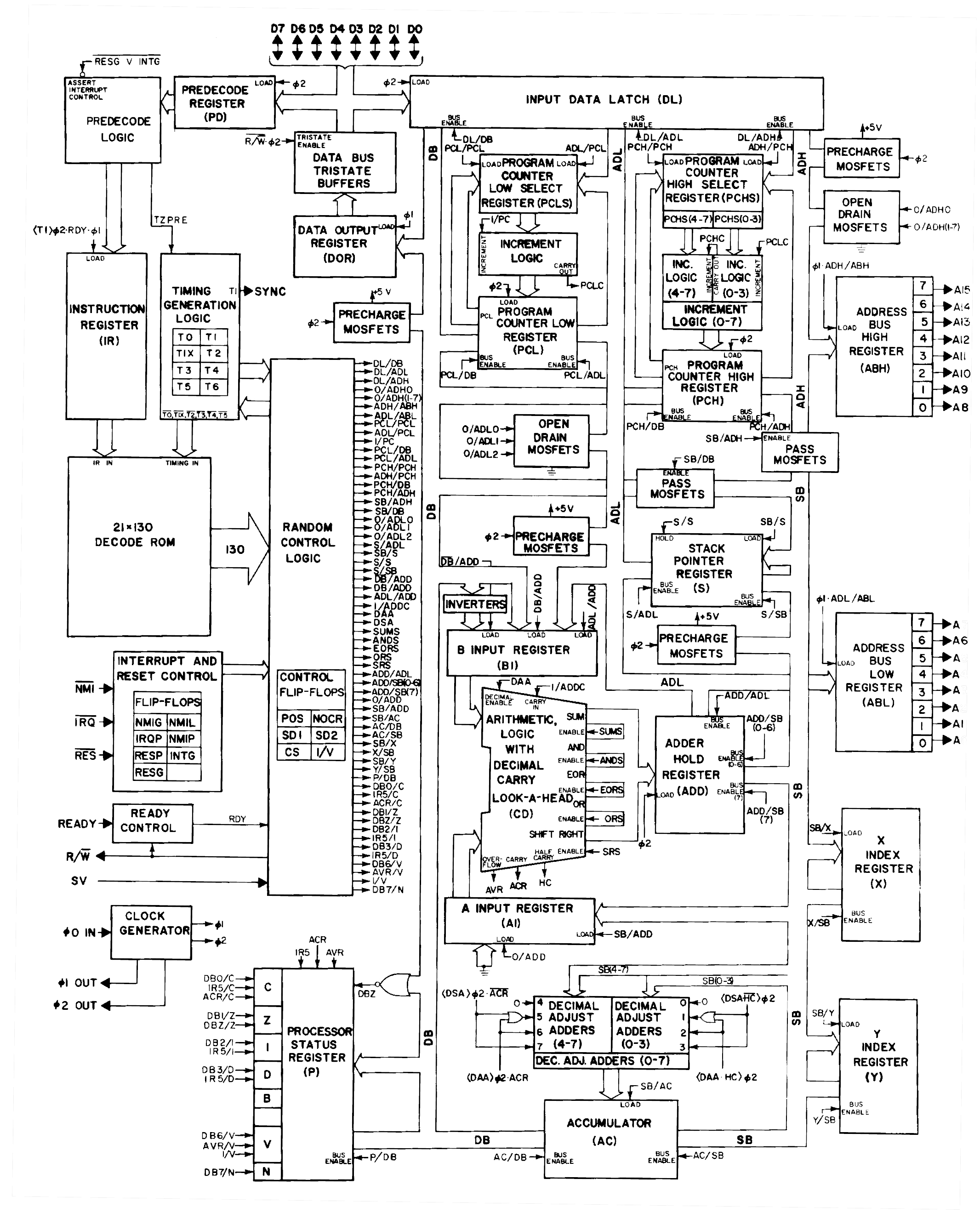
I believe I now have a working model of a 6502 Logisim circuit that (I think) will translate well to a viable hardware implementation on 7400 series chips. It’s an important milestone on my way to building a TTL 6502 and (eventually) a C64 to host it. I was a complete newb to hardware design when this crazy project started (still am really), so this is a big deal to me. My first attempt was a totally impractical design (particularly the instruction decoder and sequencer which required well over a hundred nested gates and implemented only a heavily simplified version of the 6502 instruction set – see attached pic. It actually worked but what a monster!). I suppose it would have been advisable to start this foray into hardware design with a less ambitious project. Nevertheless, this is where I’ve landed and as you may be able to tell, I like jumping into things with both feet in any case.
There is no way for me to really know what will happen when I try to get this second (and much simpler) microcode-based design onto real chips, but I can at least be optimistic. I have tried to use only elements with ready 7400 series equivalents (no crazy 12 input gates, etc.), and tried also to meet their data sheet requirements as I went. Fingers crossed on how that will go. In the meantime, so far as I can tell, the Logisim simulation I have here is fairly accurate but with some differences worth noting. Here is a summary:
• Full 6502 instruction set, including all addressing modes, registers, decimal mode and RS, NMI, and IRQ interrupts,
• Microcode implementation (I wanted a minimum number of ROMs so kept some good ol’ gate-level decoding to stay within a 32 bit control word),
• Single 50% duty-cycle clock rather than the 6502 two-phase one (have to confess to not really understanding the requirement for two non-overlapping phases vs. using a single rising-edge to clock all flip-flops. The later seems much more straight forward. Any explanation on the trade-offs here would be very much appreciated),
• Official opcodes only (all illegal opcodes are NOPs, with the exception of $FA, $FC and $FF which are used for NMI, RS and IRQ microcode sequences respectively),
• Interrupts are recognized at the beginning of the instruction cycle but ignored once a given microcode sequence has begun (the simulation will not recognize an NMI, for example, once the microcode sequence for a lower priority IRQ is in progress),
• No SYNC line implemented (although I think I might be able to use the “Write to IR” control signal almost as is for this?)
• Address and Data busses are held in high-impedance state during phase 1 of the clock to facilitate a memory mapped screen RAM design,
• /BEN (Bus ENable) input pin tri-states the busses asynchronously when high (I think this is roughly equivalent to the 6510’s AEC pin. I might just drop this given the buses are already available during phase 1),
• The RESET sequence uses the 6502 “inhibited write” spare cycles to initialize the stack pointer and clear the decimal flag,
• ADC and SBC instructions take an extra cycle to complete in decimal mode, flags are updated but I still need to validate this is done properly, (Btw, I am amazed the 6502 can fit the binary operation and the BCD adjustment in one cycle! I found I had to split this into two cycles to get anywhere near reasonable propagation delay through all the required logic),
• JMP absolute instruction takes 4 cycles rather than 3 (this would have required some otherwise redundant logic to preserve the PC after fetching the low-byte of the target address. In the end, I decided the extra cycle was worth the savings in extra data path),
• A few other instructions take fewer cycles to complete than in a standard 6502 (e.g. LSR absolute-indexed instruction takes 6 cycles rather than 7 when a page boundary is not crossed - the microcode can easily be adjusted to add dummy cycles and retain more cycle compatibility in these instances. I will likely do that before finalizing the design just to minimize differences).
The design borrows heavily from Dieter Mueller’s multiplexer ALU as well as from multiple articles and posts found on this site about decimal mode, interrupt handling and many other aspects of the 6502’s behavior. I remember thinking that there might be scraps of information on the web about this obscure processor I had programmed as a kid. Instead, I was amazed to find a vibrant community of interest eager to share and learn. The fact that I've been able to get this far is largely due to this community. Many thanks to all of you for that.
On that note, I have run Klaus’ test harness (thank you Klaus) on this simulator and it appears to pass, although truthfully I’m not sure. I’ve read this test will run for about 1 minute at 2 MHz. It will take far longer than I am prepared to wait at the dismal 100Hz Logisim achieves. Nevertheless, I have run through all tests to completion, except the binary and decimal arithmetic tests. For those, I have run through a handful of iterations only (I gave up after three days) and have been forced to rely on unit tests for the time being. A more complete test will have to wait until I have a faster implementation.
I am happy to eventually post the Logisim files if this turns out to be of interest to anyone (and provided I get permission from those I have liberally borrowed from). Of course all comments and questions are welcome. I am particularly interested in ways to validate and simplify the design before going to hardware. I’ll post up some specific questions when I get a chance. As I mentioned, I’m new to hardware so can use all the help I can get.
My best to everyone here,
Drass
P.S. moderator: I posted this on the Hardware section because that's where I am headed. Please feel free to move it to the Simulation section if appropriate.
First post here and a big day for me.
I believe I now have a working model of a 6502 Logisim circuit that (I think) will translate well to a viable hardware implementation on 7400 series chips. It’s an important milestone on my way to building a TTL 6502 and (eventually) a C64 to host it. I was a complete newb to hardware design when this crazy project started (still am really), so this is a big deal to me. My first attempt was a totally impractical design (particularly the instruction decoder and sequencer which required well over a hundred nested gates and implemented only a heavily simplified version of the 6502 instruction set – see attached pic. It actually worked but what a monster!). I suppose it would have been advisable to start this foray into hardware design with a less ambitious project. Nevertheless, this is where I’ve landed and as you may be able to tell, I like jumping into things with both feet in any case.
There is no way for me to really know what will happen when I try to get this second (and much simpler) microcode-based design onto real chips, but I can at least be optimistic. I have tried to use only elements with ready 7400 series equivalents (no crazy 12 input gates, etc.), and tried also to meet their data sheet requirements as I went. Fingers crossed on how that will go. In the meantime, so far as I can tell, the Logisim simulation I have here is fairly accurate but with some differences worth noting. Here is a summary:
• Full 6502 instruction set, including all addressing modes, registers, decimal mode and RS, NMI, and IRQ interrupts,
• Microcode implementation (I wanted a minimum number of ROMs so kept some good ol’ gate-level decoding to stay within a 32 bit control word),
• Single 50% duty-cycle clock rather than the 6502 two-phase one (have to confess to not really understanding the requirement for two non-overlapping phases vs. using a single rising-edge to clock all flip-flops. The later seems much more straight forward. Any explanation on the trade-offs here would be very much appreciated),
• Official opcodes only (all illegal opcodes are NOPs, with the exception of $FA, $FC and $FF which are used for NMI, RS and IRQ microcode sequences respectively),
• Interrupts are recognized at the beginning of the instruction cycle but ignored once a given microcode sequence has begun (the simulation will not recognize an NMI, for example, once the microcode sequence for a lower priority IRQ is in progress),
• No SYNC line implemented (although I think I might be able to use the “Write to IR” control signal almost as is for this?)
• Address and Data busses are held in high-impedance state during phase 1 of the clock to facilitate a memory mapped screen RAM design,
• /BEN (Bus ENable) input pin tri-states the busses asynchronously when high (I think this is roughly equivalent to the 6510’s AEC pin. I might just drop this given the buses are already available during phase 1),
• The RESET sequence uses the 6502 “inhibited write” spare cycles to initialize the stack pointer and clear the decimal flag,
• ADC and SBC instructions take an extra cycle to complete in decimal mode, flags are updated but I still need to validate this is done properly, (Btw, I am amazed the 6502 can fit the binary operation and the BCD adjustment in one cycle! I found I had to split this into two cycles to get anywhere near reasonable propagation delay through all the required logic),
• JMP absolute instruction takes 4 cycles rather than 3 (this would have required some otherwise redundant logic to preserve the PC after fetching the low-byte of the target address. In the end, I decided the extra cycle was worth the savings in extra data path),
• A few other instructions take fewer cycles to complete than in a standard 6502 (e.g. LSR absolute-indexed instruction takes 6 cycles rather than 7 when a page boundary is not crossed - the microcode can easily be adjusted to add dummy cycles and retain more cycle compatibility in these instances. I will likely do that before finalizing the design just to minimize differences).
The design borrows heavily from Dieter Mueller’s multiplexer ALU as well as from multiple articles and posts found on this site about decimal mode, interrupt handling and many other aspects of the 6502’s behavior. I remember thinking that there might be scraps of information on the web about this obscure processor I had programmed as a kid. Instead, I was amazed to find a vibrant community of interest eager to share and learn. The fact that I've been able to get this far is largely due to this community. Many thanks to all of you for that.
On that note, I have run Klaus’ test harness (thank you Klaus) on this simulator and it appears to pass, although truthfully I’m not sure. I’ve read this test will run for about 1 minute at 2 MHz. It will take far longer than I am prepared to wait at the dismal 100Hz Logisim achieves. Nevertheless, I have run through all tests to completion, except the binary and decimal arithmetic tests. For those, I have run through a handful of iterations only (I gave up after three days) and have been forced to rely on unit tests for the time being. A more complete test will have to wait until I have a faster implementation.
I am happy to eventually post the Logisim files if this turns out to be of interest to anyone (and provided I get permission from those I have liberally borrowed from). Of course all comments and questions are welcome. I am particularly interested in ways to validate and simplify the design before going to hardware. I’ll post up some specific questions when I get a chance. As I mentioned, I’m new to hardware so can use all the help I can get.
My best to everyone here,
Drass
P.S. moderator: I posted this on the Hardware section because that's where I am headed. Please feel free to move it to the Simulation section if appropriate.