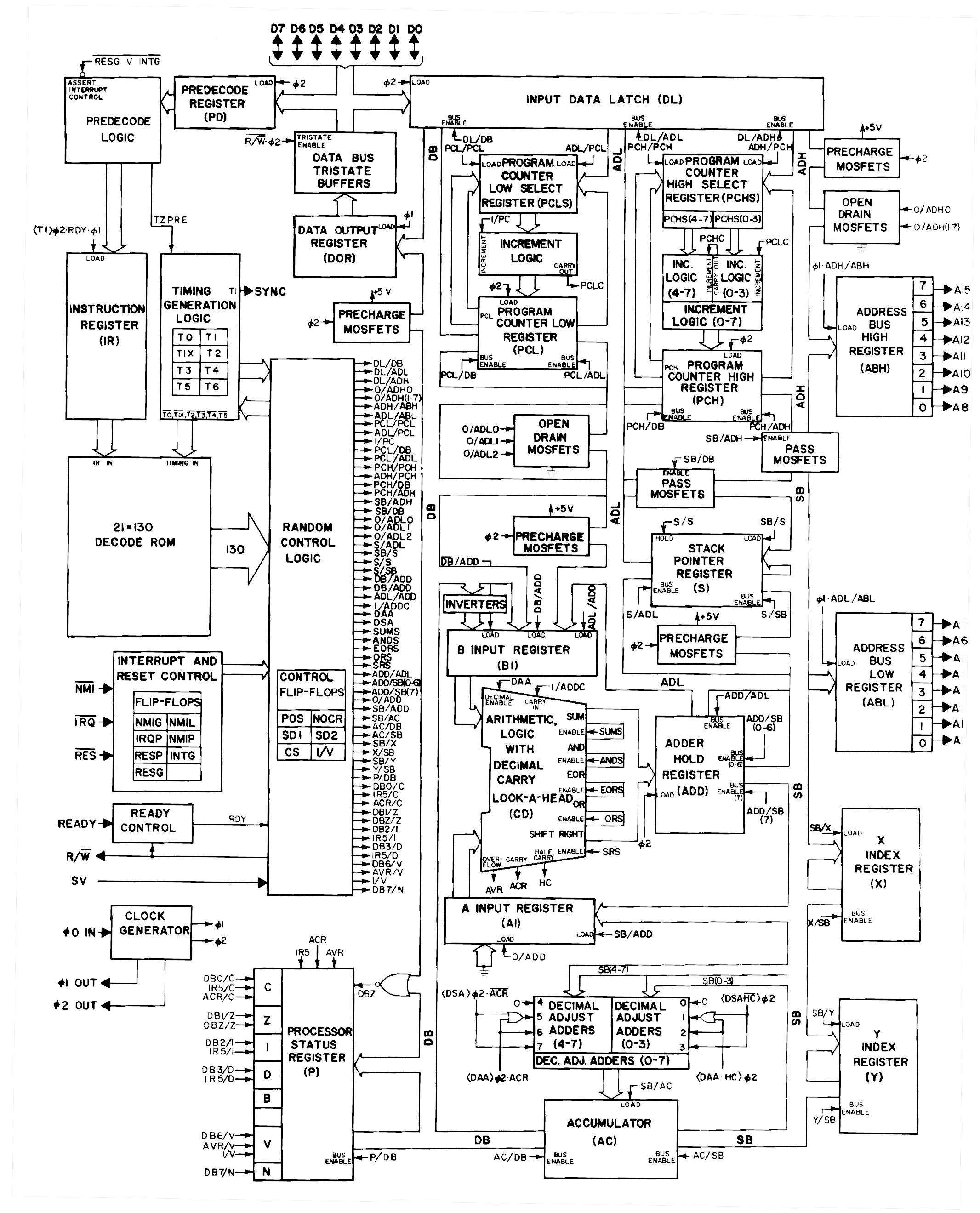
Eureka! With a transistor-level simulation of the 6502 in hand, we can see exactly what's going on cycle by cycle. (Or even phase by phase.) Huge thanks to Greg James, Barry Silverman and Brian Silverman for their
Visual6502 project (website under construction - see
other thread) which provided the simulator and the netlist.
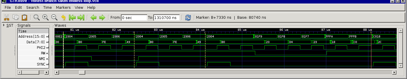
Here's a late interrupt into a taken branch, should be timed the same as the example above:
Code: Select all
testNMI(28)
 cyc:10 cp1:1 cp2:0 Add:2304 D:b0 RnW:1  PC:2304 SP:fd  Sync:1 NMI:1  IR:b0 TCstate:111111  fetch:0 clearIR:1 D1x1:1
 cyc:10 cp1:0 cp2:1 Add:2304 D:b0 RnW:1  PC:2304 SP:fd  Sync:1 NMI:1  IR:b0 TCstate:111111  fetch:1 clearIR:0 D1x1:1
 cyc:11 cp1:1 cp2:0 Add:2305 D:fe RnW:1  PC:2305 SP:fd  Sync:0 NMI:1  IR:b0 TCstate:110111  fetch:1 clearIR:0 D1x1:1
 cyc:11 cp1:0 cp2:1 Add:2305 D:fe RnW:1  PC:2305 SP:fd  Sync:0 NMI:1  IR:b0 TCstate:110111  fetch:0 clearIR:1 D1x1:1
 cyc:12 cp1:1 cp2:0 Add:2306 D:00 RnW:1  PC:2306 SP:fd  Sync:0 NMI:1  IR:b0 TCstate:111011  fetch:0 clearIR:1 D1x1:1
 cyc:12 cp1:0 cp2:1 Add:2306 D:00 RnW:1  PC:2306 SP:fd  Sync:0 NMI:1  IR:b0 TCstate:111011  fetch:0 clearIR:1 D1x1:1
 cyc:13 cp1:1 cp2:0 Add:2304 D:b0 RnW:1  PC:2304 SP:fd  Sync:1 NMI:1  IR:b0 TCstate:111111  fetch:0 clearIR:1 D1x1:1
 cyc:13 cp1:0 cp2:1 Add:2304 D:b0 RnW:1  PC:2304 SP:fd  Sync:1 NMI:1  IR:b0 TCstate:111111  fetch:1 clearIR:0 D1x1:1
 cyc:14 cp1:1 cp2:0 Add:2305 D:fe RnW:1  PC:2305 SP:fd  Sync:0 NMI:1  IR:b0 TCstate:110111  fetch:1 clearIR:0 D1x1:1
 cyc:14 cp1:1 cp2:0 Add:2305 D:fe RnW:1  PC:2305 SP:fd  Sync:0 NMI:0  IR:b0 TCstate:110111  fetch:1 clearIR:0 D1x1:1
 cyc:14 cp1:0 cp2:1 Add:2305 D:fe RnW:1  PC:2305 SP:fd  Sync:0 NMI:0  IR:b0 TCstate:110111  fetch:0 clearIR:1 D1x1:1
 cyc:15 cp1:1 cp2:0 Add:2306 D:00 RnW:1  PC:2306 SP:fd  Sync:0 NMI:0  IR:b0 TCstate:111011  fetch:0 clearIR:1 D1x1:1
 cyc:15 cp1:0 cp2:1 Add:2306 D:00 RnW:1  PC:2306 SP:fd  Sync:0 NMI:0  IR:b0 TCstate:111011  fetch:0 clearIR:1 D1x1:1
 cyc:16 cp1:1 cp2:0 Add:2304 D:b0 RnW:1  PC:2304 SP:fd  Sync:1 NMI:0  IR:b0 TCstate:111111  fetch:0 clearIR:1 D1x1:1
 cyc:16 cp1:0 cp2:1 Add:2304 D:b0 RnW:1  PC:2304 SP:fd  Sync:1 NMI:0  IR:b0 TCstate:111111  fetch:1 clearIR:0 D1x1:1
 cyc:17 cp1:1 cp2:0 Add:2305 D:fe RnW:1  PC:2305 SP:fd  Sync:0 NMI:0  IR:b0 TCstate:110111  fetch:1 clearIR:0 D1x1:1
 cyc:17 cp1:0 cp2:1 Add:2305 D:fe RnW:1  PC:2305 SP:fd  Sync:0 NMI:0  IR:b0 TCstate:110111  fetch:0 clearIR:1 D1x1:0
 cyc:18 cp1:1 cp2:0 Add:2306 D:00 RnW:1  PC:2306 SP:fd  Sync:0 NMI:0  IR:b0 TCstate:111011  fetch:0 clearIR:1 D1x1:0
 cyc:18 cp1:1 cp2:0 Add:2306 D:00 RnW:1  PC:2306 SP:fd  Sync:0 NMI:1  IR:b0 TCstate:111011  fetch:0 clearIR:1 D1x1:0
 cyc:18 cp1:0 cp2:1 Add:2306 D:00 RnW:1  PC:2306 SP:fd  Sync:0 NMI:1  IR:b0 TCstate:111011  fetch:0 clearIR:1 D1x1:0
 cyc:19 cp1:1 cp2:0 Add:2304 D:b0 RnW:1  PC:2304 SP:fd  Sync:1 NMI:1  IR:b0 TCstate:111111  fetch:0 clearIR:1 D1x1:0
 cyc:19 cp1:0 cp2:1 Add:2304 D:b0 RnW:1  PC:2304 SP:fd  Sync:1 NMI:1  IR:b0 TCstate:111111  fetch:1 clearIR:1 D1x1:0
 cyc:20 cp1:1 cp2:0 Add:2304 D:b0 RnW:1  PC:2304 SP:fd  Sync:0 NMI:1  IR:00 TCstate:110111  fetch:1 clearIR:1 D1x1:0
 cyc:20 cp1:0 cp2:1 Add:2304 D:b0 RnW:1  PC:2304 SP:fd  Sync:0 NMI:1  IR:00 TCstate:110111  fetch:0 clearIR:1 D1x1:0
 cyc:21 cp1:1 cp2:0 Add:01fd D:b0 RnW:0  PC:2304 SP:fd  Sync:0 NMI:1  IR:00 TCstate:111011  fetch:0 clearIR:1 D1x1:0
 cyc:21 cp1:0 cp2:1 Add:01fd D:23 RnW:0  PC:2304 SP:fd  Sync:0 NMI:1  IR:00 TCstate:111011  fetch:0 clearIR:1 D1x1:0
Here's a trace of the simulator's test program:
Code: Select all
 cyc:2 cp1:1 cp2:0 Add:0000 D:a9 RnW:1  PC:0000 SP:fd  Sync:1 NMI:1  IR:00 TCstate:011111  fetch:0 clearIR:1 D1x1:1
 cyc:2 cp1:0 cp2:1 Add:0000 D:a9 RnW:1  PC:0000 SP:fd  Sync:1 NMI:1  IR:00 TCstate:011111  fetch:1 clearIR:0 D1x1:1
 cyc:3 cp1:1 cp2:0 Add:0001 D:00 RnW:1  PC:0001 SP:fd  Sync:0 NMI:1  IR:a9 TCstate:100111  fetch:1 clearIR:0 D1x1:1
 cyc:3 cp1:0 cp2:1 Add:0001 D:00 RnW:1  PC:0001 SP:fd  Sync:0 NMI:1  IR:a9 TCstate:100111  fetch:0 clearIR:1 D1x1:1
 cyc:4 cp1:1 cp2:0 Add:0002 D:20 RnW:1  PC:0002 SP:fd  Sync:1 NMI:1  IR:a9 TCstate:011111  fetch:0 clearIR:1 D1x1:1
 cyc:4 cp1:0 cp2:1 Add:0002 D:20 RnW:1  PC:0002 SP:fd  Sync:1 NMI:1  IR:a9 TCstate:011111  fetch:1 clearIR:0 D1x1:1
 cyc:5 cp1:1 cp2:0 Add:0003 D:10 RnW:1  PC:0003 SP:fd  Sync:0 NMI:1  IR:20 TCstate:110111  fetch:1 clearIR:0 D1x1:1
 cyc:5 cp1:0 cp2:1 Add:0003 D:10 RnW:1  PC:0003 SP:fd  Sync:0 NMI:1  IR:20 TCstate:110111  fetch:0 clearIR:1 D1x1:1
 cyc:6 cp1:1 cp2:0 Add:01fd D:00 RnW:1  PC:0004 SP:10  Sync:0 NMI:1  IR:20 TCstate:111011  fetch:0 clearIR:1 D1x1:1
 cyc:6 cp1:0 cp2:1 Add:01fd D:00 RnW:1  PC:0004 SP:10  Sync:0 NMI:1  IR:20 TCstate:111011  fetch:0 clearIR:1 D1x1:1
 cyc:7 cp1:1 cp2:0 Add:01fd D:00 RnW:0  PC:0004 SP:10  Sync:0 NMI:1  IR:20 TCstate:111101  fetch:0 clearIR:1 D1x1:1
 cyc:7 cp1:0 cp2:1 Add:01fd D:00 RnW:0  PC:0004 SP:10  Sync:0 NMI:1  IR:20 TCstate:111101  fetch:0 clearIR:1 D1x1:1
 cyc:8 cp1:1 cp2:0 Add:01fc D:00 RnW:0  PC:0004 SP:10  Sync:0 NMI:1  IR:20 TCstate:111110  fetch:0 clearIR:1 D1x1:1
 cyc:8 cp1:0 cp2:1 Add:01fc D:04 RnW:0  PC:0004 SP:10  Sync:0 NMI:1  IR:20 TCstate:111110  fetch:0 clearIR:1 D1x1:1
 cyc:9 cp1:1 cp2:0 Add:0004 D:00 RnW:1  PC:0004 SP:10  Sync:0 NMI:1  IR:20 TCstate:101111  fetch:0 clearIR:1 D1x1:1
 cyc:9 cp1:0 cp2:1 Add:0004 D:00 RnW:1  PC:0004 SP:10  Sync:0 NMI:1  IR:20 TCstate:101111  fetch:0 clearIR:1 D1x1:1
Now we know exactly what happens, we just need to figure out why! And we can trace any signal on the chip, so long as we can find it. (We can also add and remove transistors if that seems appealling. There are only 3510 transistors there - all the pullups are modelled separately.)
My current thinking is that the succession of Tstates for a normal instruction stream visits 101111 in the last cycle of an instruction, and this is when the interrupt handler kicks off. Taken branches never visit 101111 - they sort of interrupt themselves - and so they wouldn't be interruptible if it weren't for the special handling.
We can see that an interrupt acts differently by watching the Tstates as an interrupt is taken - we don't visit 011111
Code: Select all
  cyc:7 cp1:1 cp2:0 Add:2306 D:b0 RnW:1  PC:2306 SP:fd  Sync:1 NMI:1  IR:4c TCstate:011111  fetch:0 clearIR:1 D1x1:1
  cyc:7 cp1:0 cp2:1 Add:2306 D:b0 RnW:1  PC:2306 SP:fd  Sync:1 NMI:1  IR:4c TCstate:011111  fetch:1 clearIR:0 D1x1:1
  cyc:8 cp1:1 cp2:0 Add:2307 D:01 RnW:1  PC:2307 SP:fd  Sync:0 NMI:1  IR:b0 TCstate:110111  fetch:1 clearIR:0 D1x1:1
  cyc:8 cp1:0 cp2:1 Add:2307 D:01 RnW:1  PC:2307 SP:fd  Sync:0 NMI:1  IR:b0 TCstate:110111  fetch:0 clearIR:1 D1x1:1
  cyc:9 cp1:1 cp2:0 Add:2308 D:00 RnW:1  PC:2308 SP:fd  Sync:0 NMI:1  IR:b0 TCstate:111011  fetch:0 clearIR:1 D1x1:1
  cyc:9 cp1:0 cp2:1 Add:2308 D:00 RnW:1  PC:2308 SP:fd  Sync:0 NMI:1  IR:b0 TCstate:111011  fetch:0 clearIR:1 D1x1:1
 cyc:10 cp1:1 cp2:0 Add:2309 D:a9 RnW:1  PC:2309 SP:fd  Sync:1 NMI:1  IR:b0 TCstate:111111  fetch:0 clearIR:1 D1x1:1
 cyc:10 cp1:0 cp2:1 Add:2309 D:a9 RnW:1  PC:2309 SP:fd  Sync:1 NMI:1  IR:b0 TCstate:111111  fetch:1 clearIR:0 D1x1:1
 cyc:11 cp1:1 cp2:0 Add:230a D:de RnW:1  PC:230a SP:fd  Sync:0 NMI:1  IR:a9 TCstate:100111  fetch:1 clearIR:0 D1x1:1
 cyc:11 cp1:0 cp2:1 Add:230a D:de RnW:1  PC:230a SP:fd  Sync:0 NMI:1  IR:a9 TCstate:100111  fetch:0 clearIR:1 D1x1:1
followed here by another which crosses a page boundary:
Code: Select all
 cyc:12 cp1:1 cp2:0 Add:230b D:b0 RnW:1  PC:230b SP:fd  Sync:1 NMI:1  IR:a9 TCstate:011111  fetch:0 clearIR:1 D1x1:1
 cyc:12 cp1:0 cp2:1 Add:230b D:b0 RnW:1  PC:230b SP:fd  Sync:1 NMI:1  IR:a9 TCstate:011111  fetch:1 clearIR:0 D1x1:1
 cyc:13 cp1:1 cp2:0 Add:230c D:f2 RnW:1  PC:230c SP:fd  Sync:0 NMI:1  IR:b0 TCstate:110111  fetch:1 clearIR:0 D1x1:1
 cyc:13 cp1:0 cp2:1 Add:230c D:f2 RnW:1  PC:230c SP:fd  Sync:0 NMI:1  IR:b0 TCstate:110111  fetch:0 clearIR:1 D1x1:1
 cyc:14 cp1:1 cp2:0 Add:230d D:00 RnW:1  PC:230d SP:fd  Sync:0 NMI:1  IR:b0 TCstate:111011  fetch:0 clearIR:1 D1x1:1
 cyc:14 cp1:0 cp2:1 Add:230d D:00 RnW:1  PC:230d SP:fd  Sync:0 NMI:1  IR:b0 TCstate:111011  fetch:0 clearIR:1 D1x1:1
 cyc:15 cp1:1 cp2:0 Add:23ff D:00 RnW:1  PC:23ff SP:fd  Sync:0 NMI:1  IR:b0 TCstate:101111  fetch:0 clearIR:1 D1x1:1
 cyc:15 cp1:0 cp2:1 Add:23ff D:00 RnW:1  PC:23ff SP:fd  Sync:0 NMI:1  IR:b0 TCstate:101111  fetch:0 clearIR:1 D1x1:1
 cyc:16 cp1:1 cp2:0 Add:22ff D:38 RnW:1  PC:22ff SP:fd  Sync:1 NMI:1  IR:b0 TCstate:011111  fetch:0 clearIR:1 D1x1:1
 cyc:16 cp1:0 cp2:1 Add:22ff D:38 RnW:1  PC:22ff SP:fd  Sync:1 NMI:1  IR:b0 TCstate:011111  fetch:1 clearIR:0 D1x1:1
in which case the branch does visit the final state 101111 and the next instruction does start with a 011111 as usual.
A branch may be a case a bit like an indexed write where the final instruction state must be reserved in case a page is crossed. In the case of a branch, the next instruction isn't known to have started until it's known that there's no page crossing. The following instruction after a taken branch doesn't have a normal first cycle. And so a taken branch doesn't have a 'final' state, and so it wouldn't be interruptible. Instead it begins the interrupt handler during T2, which means the NMI needs to enter the chip a bit earlier than the usual case in order to catch the window. We see that the other way around: the interrupt appears to have been deferred.
Hope this makes some degree of sense!
Cheers
Ed

