
Hi Garth
Michael Steil says that the normal interrupt sequence is followed - there are three stack accesses - but that RnW stays high, so there are no writes.
Do you believe you saw writes, or did you just see the addresses?
(I'm interested in this because I want to trace the part of the design which adjusts RnW.)
Cheers
Ed
ps. I'm not sure yet I agree with his statement "When a 6502 is turned on, the stack pointer is initialized with zero." but I haven't yet run this case through visual6502.
65816 C64 With Discrete Instead of PAL
-
GARTHWILSON

- Forum Moderator
- Posts: 8775
- Joined: 30 Aug 2002
- Location: Southern California
- Contact:
Quote:
Michael Steil says that the normal interrupt sequence is followed - there are three stack accesses - but that RnW stays high, so there are no writes.
Do you believe you saw writes, or did you just see the addresses?
Do you believe you saw writes, or did you just see the addresses?
Quote:
ps. I'm not sure yet I agree with his statement "When a 6502 is turned on, the stack pointer is initialized with zero."
In school in 1982 we were taught to always initialize it in the reset routine. That was on the NMOS 6502 but what I find in WDC's data sheet is "All Registers are initialized by software except the Decimal and Interrupt disable mode select bits of the Processor Status Register (P) [which] are initialized by hardware." (page 11). IOW, your reset routine has to initialize all but the D and I flags.
If you leave the entire page 1 of a 6502 for the stack, it wouldn't really matter if you initialize it, because there won't be anything to overwrite; but my own tests have shown that I don't need anywhere near that much stack space even with heavy use of subroutines and interrupts; so I use some of page 1 for variables and of course the stack must be kept in its place to avoid stepping on them. [Edit, years later: There is another good reason to initialize the stack pointer, which is to make sure you don't accidentally index into page 2 if the stack wraps. More on this in my stacks treatise, starting in the middle of page 4 on stack addressing, at http://wilsonminesco.com/stacks/stackaddressing.html .]
http://WilsonMinesCo.com/ lots of 6502 resources
The "second front page" is http://wilsonminesco.com/links.html .
What's an additional VIA among friends, anyhow?
The "second front page" is http://wilsonminesco.com/links.html .
What's an additional VIA among friends, anyhow?
-
GARTHWILSON
- Forum Moderator
- Posts: 8775
- Joined: 30 Aug 2002
- Location: Southern California
- Contact:
BTW, when I did my single-cycling test mentioned above, that was on a Rockwell 65c02, not WDC, but it agreed with WDC's data sheet.
http://WilsonMinesCo.com/ lots of 6502 resources
The "second front page" is http://wilsonminesco.com/links.html .
What's an additional VIA among friends, anyhow?
The "second front page" is http://wilsonminesco.com/links.html .
What's an additional VIA among friends, anyhow?
GARTHWILSON wrote:
I'm sure I saw writes (ie, R/W\ was low) but I'd have to dig it up to be more than 90% sure. The WDC manual also says they are writes, with R/W\ low.
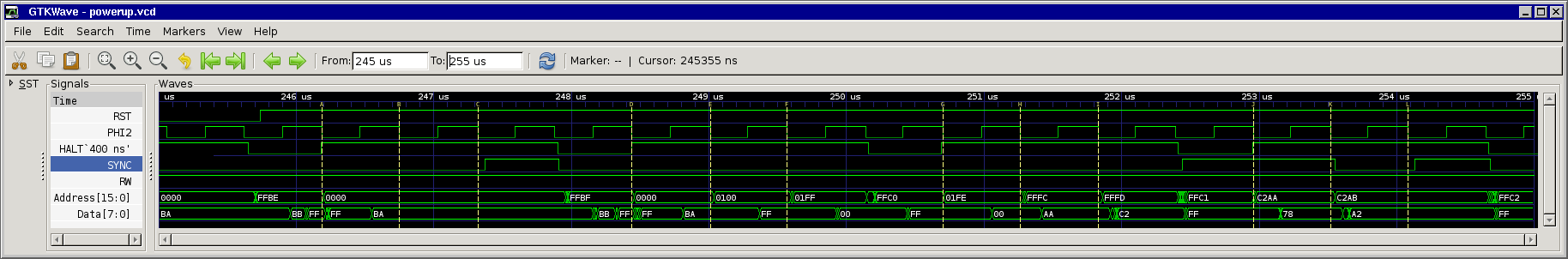
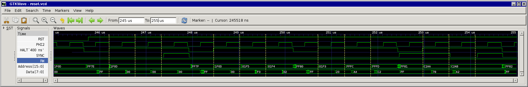
After Michael's blog post I was very interested about seeing this in action so I hooked up my logic analyzer to my Atari 800XL and captured some traces.
Unfortunately Antic dram refreshes destroy the nice pics, just ignore all cycles where HALT is low (in the pics I shifted halt by 400ns so that it's in sync with the stopped clock cycles). To make the actual CPU cycles easier to recognize I set a marker at the start of each CPU cycle.
Here's the powerup:
And here's the reset:
I hope that I'm able to capture traces of the 65C02 in a few weeks, a friend was so kind to send me a few 65C02s, now I only need the adapter board.
so long,
Hias
-
BigDumbDinosaur

- Posts: 9428
- Joined: 28 May 2009
- Location: Midwestern USA (JB Pritzker’s dystopia)
- Contact:
digidice wrote:
there is a 74F138 but no 74ABT138
Quote:
#5 A AND gate from /Ø2 and RWB to the /WE on the SRAM? That should qualify?
Quote:
#6 You say Potato, I say Potàto.  I can put GND signals in there it it makes it easier for everyone.
x86? We ain't got no x86. We don't NEED no stinking x86!
-
BigDumbDinosaur
- Posts: 9428
- Joined: 28 May 2009
- Location: Midwestern USA (JB Pritzker’s dystopia)
- Contact:
GARTHWILSON wrote:
Quote:
Okay, details man! Details!
NS access times? Cost?
NS access times? Cost?
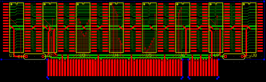
The above is on a two-layer board and accepts 512K x 8 SRAM in SOJ32 packaging. I also have a 4-layer design that is very similar. In both cases, the SIMM fits into the same card-edge receptacle that accepts 32 bit PCI cards. Four of these would fully populate an '816 system with 16 MB of static RAM.
x86? We ain't got no x86. We don't NEED no stinking x86!
-
BigDumbDinosaur
- Posts: 9428
- Joined: 28 May 2009
- Location: Midwestern USA (JB Pritzker’s dystopia)
- Contact:
GARTHWILSON wrote:
Quote:
Quote:
What's the purpose of IC5?
Quote:
digidice, it's great that you're diving into this head first, but I'm thinking it might not be a bad idea for you to make your first computer simpler. Our first efforts tend to be overblown which makes them hard to complete at all, either because we bit off more than we could chew, or after it's built we find it has problems we don't yet have the knowledge to fix or problems that can't be fixed without starting over on part of it.
Now that I have that basic unit done and running (it's very stable), I can expand on it some more. I'll give a hint of what's next: I acquired some 53C94 SCSI controller ASICs in PLCC84 packages and have the complete 'C94 data sheet.
x86? We ain't got no x86. We don't NEED no stinking x86!
-
GARTHWILSON
- Forum Moderator
- Posts: 8775
- Joined: 30 Aug 2002
- Location: Southern California
- Contact:
Quote:
How about something like this?
http://WilsonMinesCo.com/ lots of 6502 resources
The "second front page" is http://wilsonminesco.com/links.html .
What's an additional VIA among friends, anyhow?
The "second front page" is http://wilsonminesco.com/links.html .
What's an additional VIA among friends, anyhow?
-
BigDumbDinosaur
- Posts: 9428
- Joined: 28 May 2009
- Location: Midwestern USA (JB Pritzker’s dystopia)
- Contact:
GARTHWILSON wrote:
Quote:
How about something like this?
x86? We ain't got no x86. We don't NEED no stinking x86!
-
GARTHWILSON
- Forum Moderator
- Posts: 8775
- Joined: 30 Aug 2002
- Location: Southern California
- Contact:
Quote:
I looked at using posts/receptacles and card edge, and decided on the latter because of theoretically lower distributed capacitance.
Edit: In our products we have also used some really short pins and sockets where height was super limited. Those would further reduce both inductance and capacitance, but I won't use them on this because it is too easy for the user to damage them by not pulling the module out straight. Then of course there are the smaller 2mm ones and even .050" but those won't go into standard perfboard with ten holes per inch.
http://WilsonMinesCo.com/ lots of 6502 resources
The "second front page" is http://wilsonminesco.com/links.html .
What's an additional VIA among friends, anyhow?
The "second front page" is http://wilsonminesco.com/links.html .
What's an additional VIA among friends, anyhow?
-
BigDumbDinosaur
- Posts: 9428
- Joined: 28 May 2009
- Location: Midwestern USA (JB Pritzker’s dystopia)
- Contact:
GARTHWILSON wrote:
Quote:
I looked at using posts/receptacles and card edge, and decided on the latter because of theoretically lower distributed capacitance.
Another consideration of using edge connections as opposed to pins is if the pin header is on the motherboard (as it appears you are planning) then the mating receptacle has to be mounted to the memory module, which might complicate the physical construction. With edge connections, nothing has to be attached to the memory module PCB except the components. With a four-layer module, it should be possible to eliminate decoupling capacitors, since the power and ground planes act as the plates of a large capacitor.
I recall the days when memory was sold as SIPs, which plugged into a receptacle on the motherboard. Aside from the ease at which the pins could be broken off a SIP, it was discovered that the receptacle introduced undesirable reactive effects. You don't see SIP memory modules anymore. I'm sure the industry would have stayed with them if it produced better (and less expensive) results. Either way, a receptacle of some kind will be required.
x86? We ain't got no x86. We don't NEED no stinking x86!
Way off topic, but I can foresee a future where proximity connections are the wave of the future. Cheaper (no connectors) and potentially just as fast (near-field B-field communications emit much less RF than anything resembling radio antennas, which means you don't need as much shielding and no FCC license), the only hard requirement would be your components remaining within some finite distance of each other.
BDD and Garth, what I love about your arguments is that you have two experienced digital electronics engineers duking it out on the intellectual battlefield of experience, and everyone else in the galleries just sucks up bits of crumpled experience here and there, hopefully synthesizing a bigger, more complete synthesis of information useful for future projects. I know *I* am benefiting from this.
BDD and Garth, what I love about your arguments is that you have two experienced digital electronics engineers duking it out on the intellectual battlefield of experience, and everyone else in the galleries just sucks up bits of crumpled experience here and there, hopefully synthesizing a bigger, more complete synthesis of information useful for future projects. I know *I* am benefiting from this.
-
BigDumbDinosaur
- Posts: 9428
- Joined: 28 May 2009
- Location: Midwestern USA (JB Pritzker’s dystopia)
- Contact:
kc5tja wrote:
BDD and Garth, what I love about your arguments is that you have two experienced digital electronics engineers duking it out on the intellectual battlefield of experience...
As for the "duking it out" part, it's a war in which the opposing forces run around pointing sawed-off broom handles at each other and yelling "Bang! Bang!" When they're worn out from running and yelling they all go to the local tavern and swill beer together.
x86? We ain't got no x86. We don't NEED no stinking x86!

GARTHWILSON wrote:
I'm sure I saw writes (ie, R/W\ was low) but I'd have to dig it up to be more than 90% sure. The WDC manual also says they are writes, with R/W\ low.
viewtopic.php?p=2959#2959