6502.org Forum  Projects  Code  Documents  Tools  Forum
It is currently Thu Apr 25, 2024 4:32 pm

All times are UTC


Post new topic Reply to topic  [ 564 posts ]  Go to page 1, 2, 3, 4, 5 ... 38  Next
Author Message
 Post subject: POC Computer Version One
PostPosted: Tue Oct 20, 2009 2:07 am 
Offline
User avatar

Joined: Thu May 28, 2009 9:46 pm
Posts: 8143
Location: Midwestern USA
For activity related to POC V1.2, please go here.

For activity related to POC V1.3, please go here.

For activity related to POC V1.4, please go here.
———————————————————————————————————————————————————————————————
POC = Proof of Concept

I’ve been working with electronics since the late 1950s and on computer hardware since 1970.  However, I’ve never scratch-built a computer.  So here’s the first try.

Assuming this things actually flies, I will then work on developing a more ambitious system that might actually be useful for something other than holding down my workbench (beats me what that something might be, though).  However, I’m a firm believer in learning how to make a single-engine plane fly before building that four-engine jumbo jet.

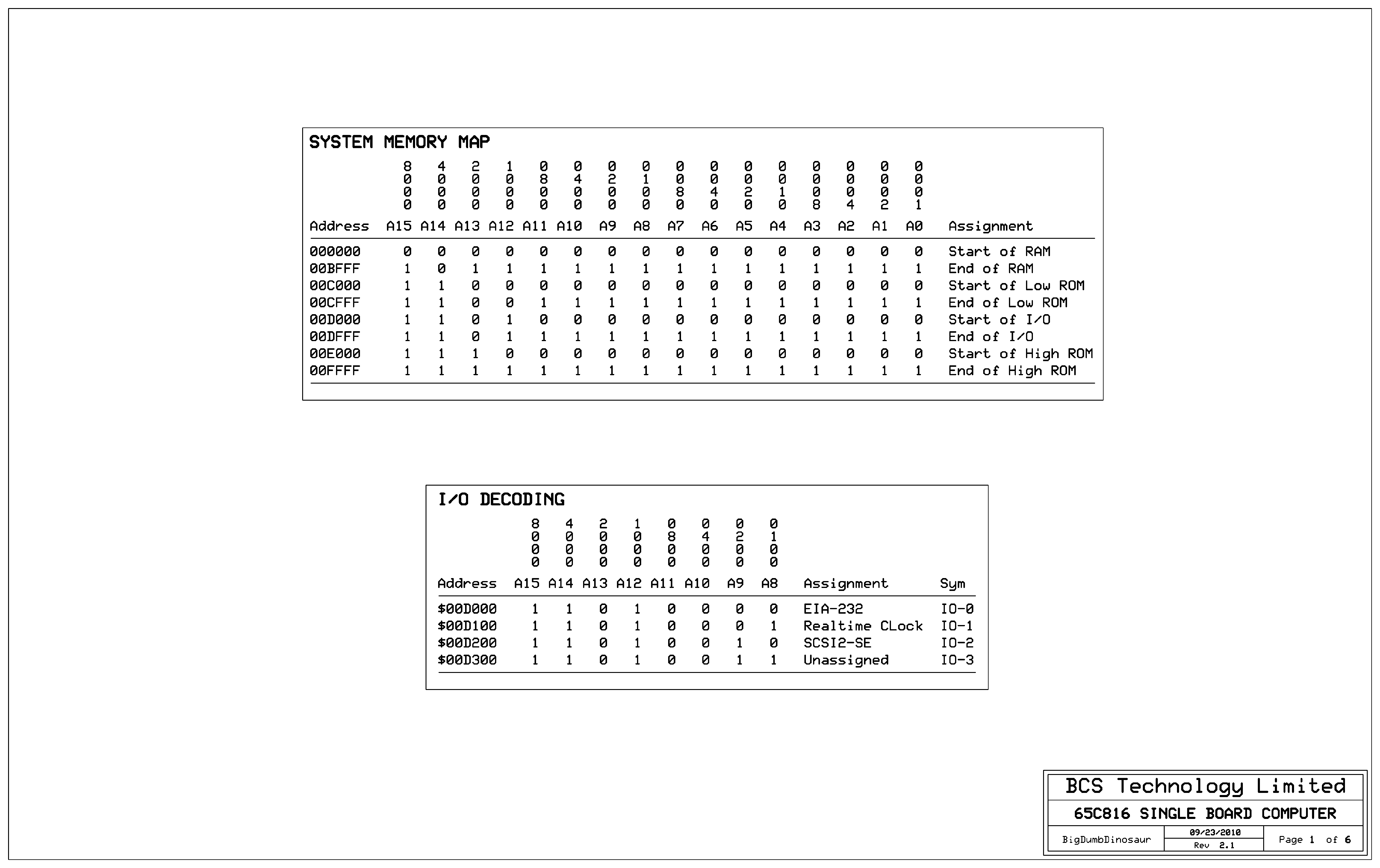
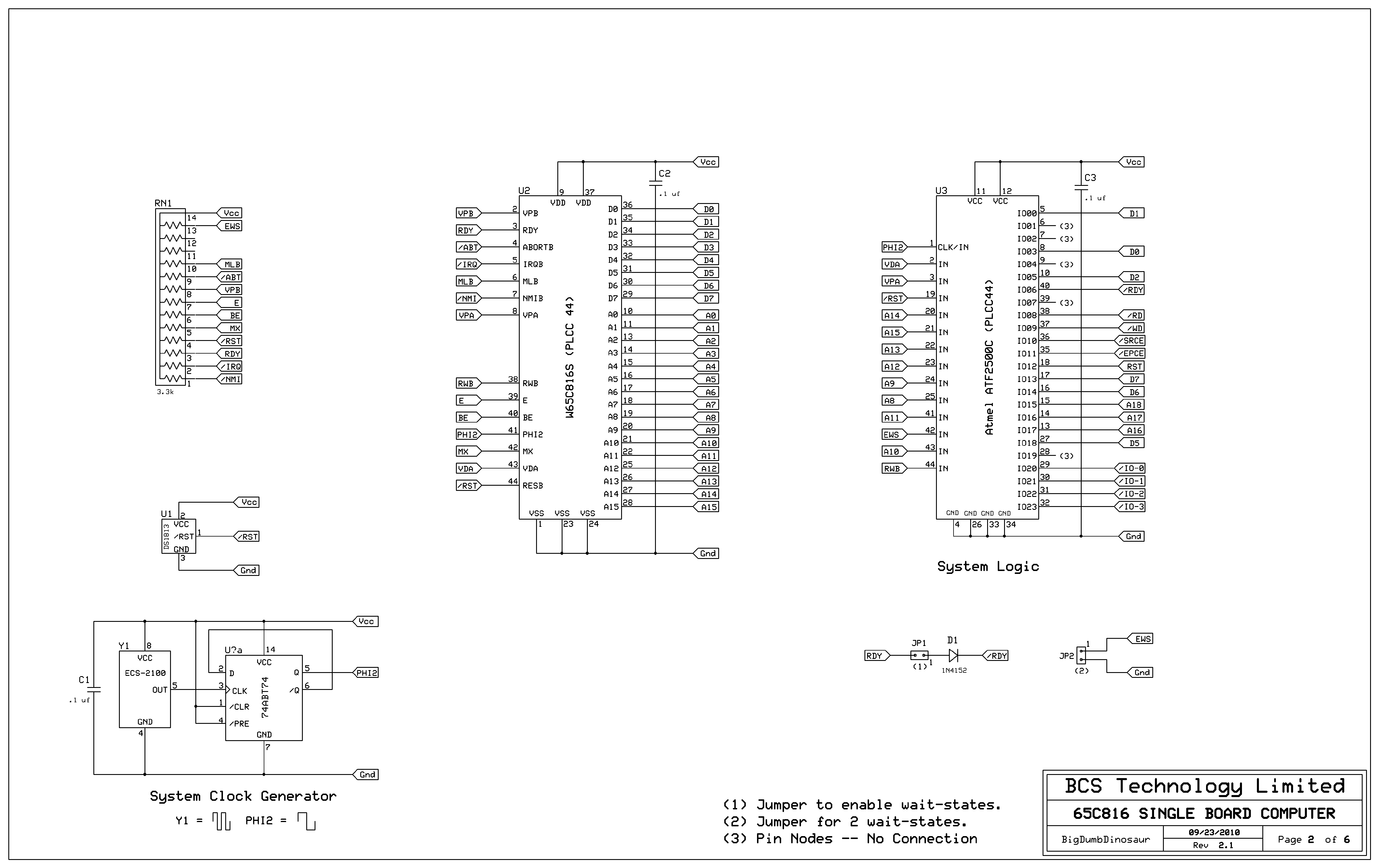
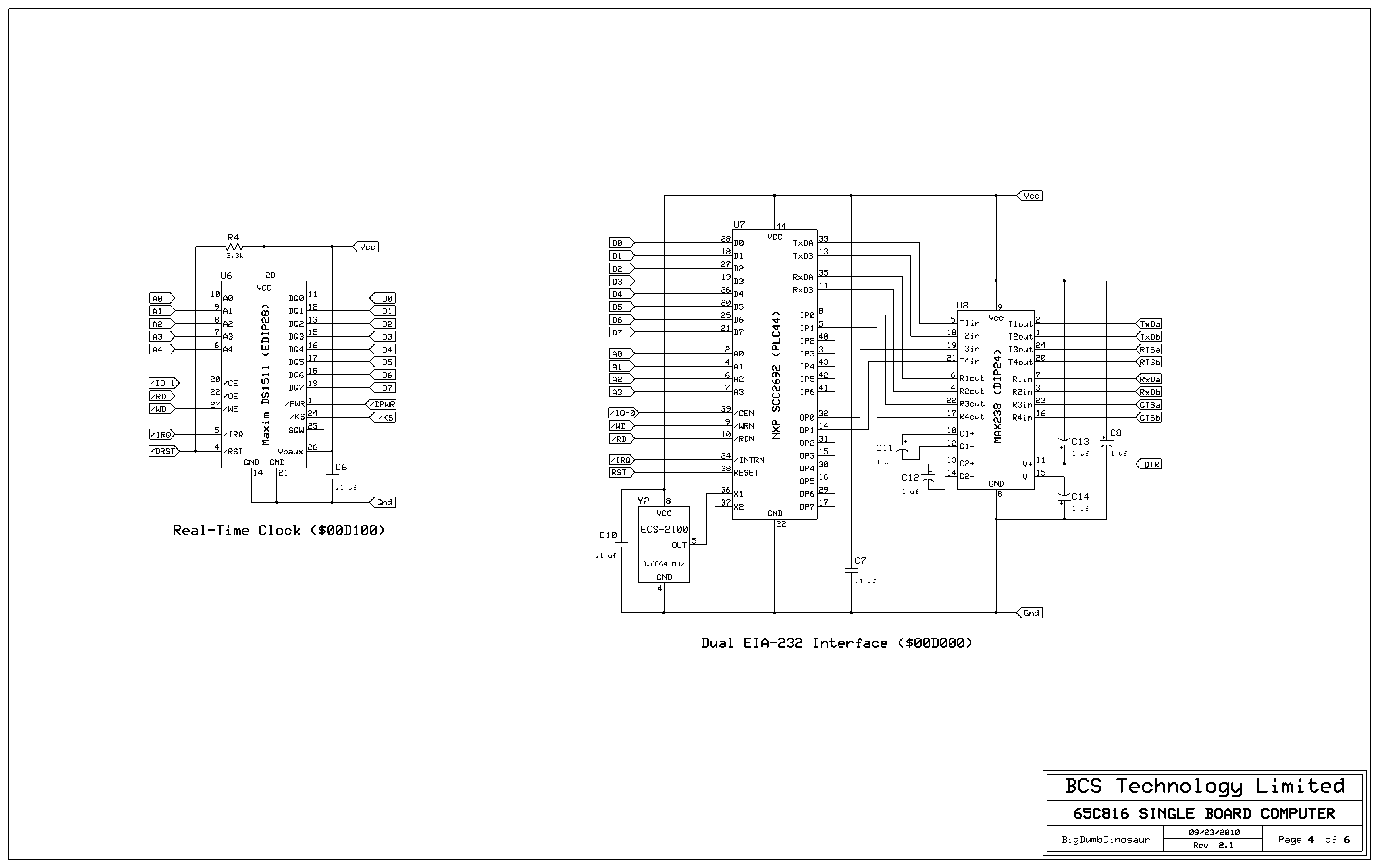
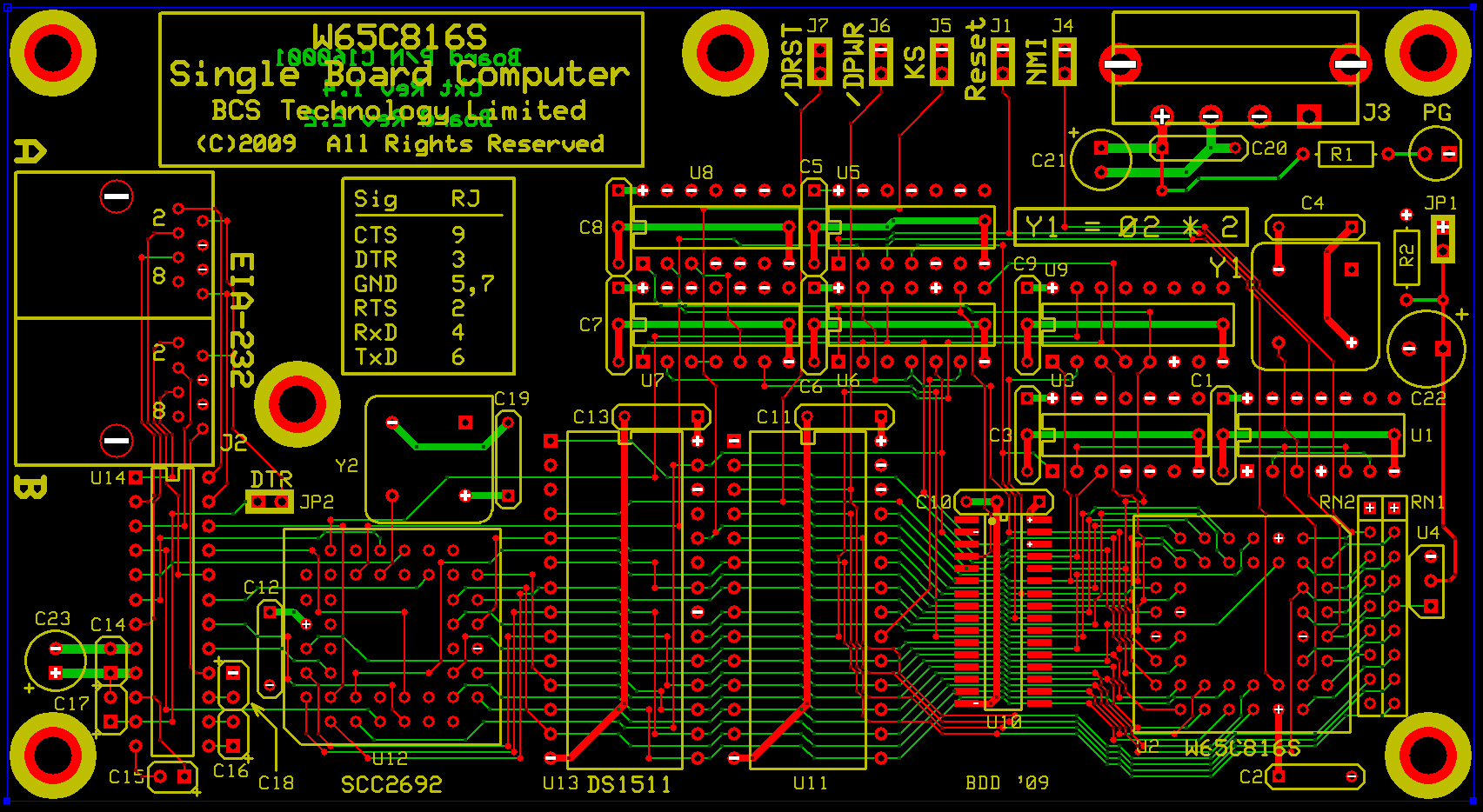
The hardware consists of a W65C816S MPU, 52K of addressable RAM, 8K of addressable ROM, an NXP 2692 dual ACIA (aka “DUART”) talking with a MAX238 line driver, and a Dallas Semi DS1511 real-time clock.  The latter has a watchdog timer, as well as a TOD clock, calendar and NVRAM.  The watchdog can be arranged to generate periodic interrupts, with a period as short as 10ms.  This would make it a natural source for a jiffy IRQ in a multitasking system...in a later design, of course.

The 2692 ACIA has two independent channels, each of which can be run at speeds up to 115.2 Kbps if desired.  TIA-232 (aka RS-232) outputs are presented at a dual 8P8C jack wired to conform with the arrangement used with Equinox SST serial interface units.  This hookup will permit me to attach one of my old WYSE 60 terminals to serial port A to act as a console.  Serial port B can be used to talk with another machine, e.g., my UNIX software development system.

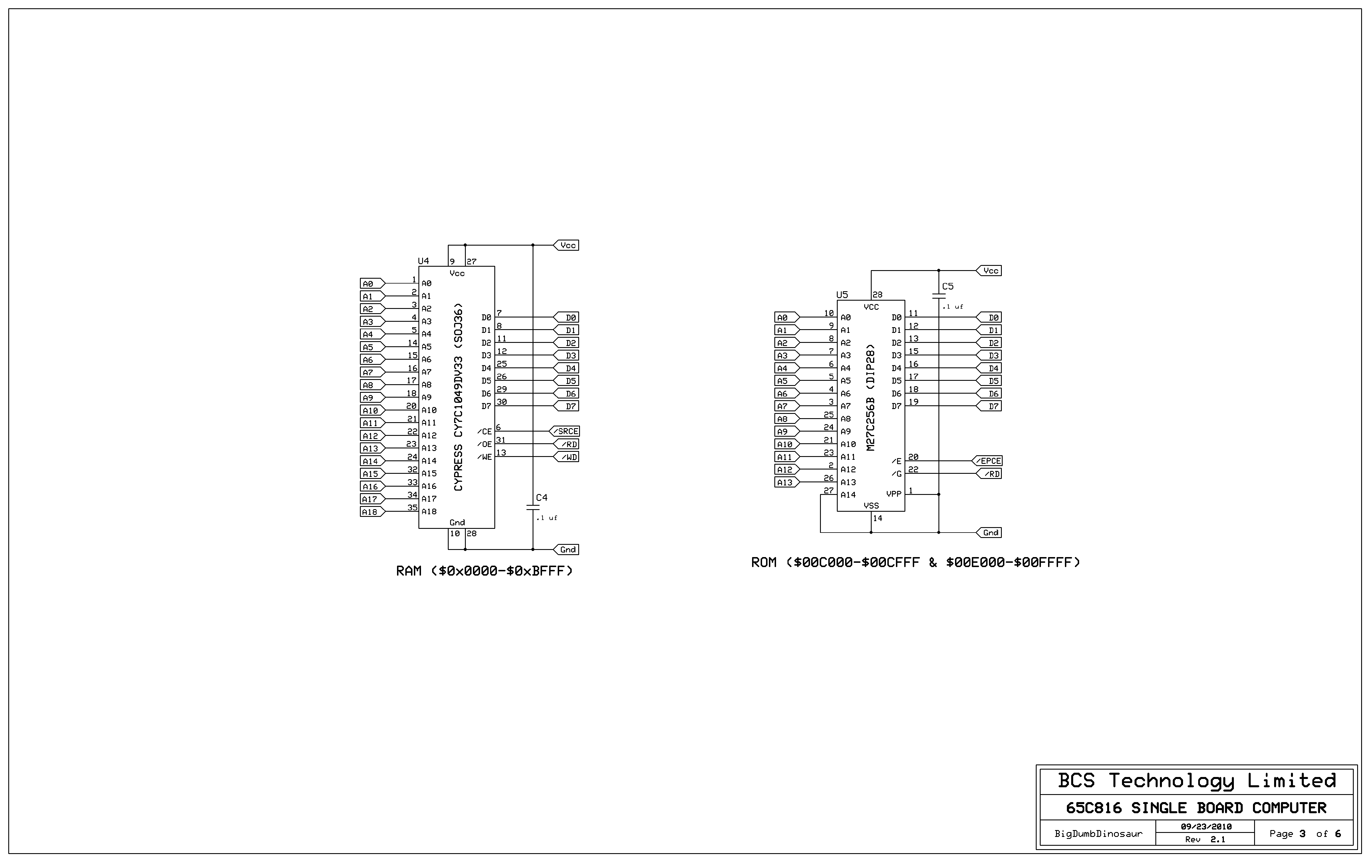
The SRAM is actually a 128KB × 8 piece that is fast (12ns) and inexpensive.  Obviously, I’m “wasting” over half of the address space, but so be it.  I’m also “wasting” ROM space, as I’m using a 32Kb by 8 EPROM (I have a bunch laying around).  However, I’m sure the ROM won’t complain.

There’s no rocket science in this design and, at least on paper, it seems it should work.  All glue logic is 74AC to keep gate propagation delays from sabotaging timing.  To assure a strong clock with real sharp rise and fall time, I’m feeding an HCMOS oscillator into a flip-flop and using the flop’s outputs to produce the actual clock.

Initial testing will be done with a 2 MHz oscillator to produce a 1 MHz Ø2 clock, as well as a NOP generator.  Once the logic probe and ’scope confirm that the thing is upright with a pulse, I’ll insert a faster oscillator.  Based upon my timing analysis, it should be stable beyond 8 MHz (16 MHz oscillator), although the 2692 DUART may have trouble at this speed (NB: such proved to be the case, and I subsequently replaced it with the faster NXP 26C92).  I will try running it faster, of course, just to see what might happen.

Here are the schematics to this mess:


I plan to build this thing on a four-layer PCB, using ExpressPCB’s ProtoPro service.  The four-layer design does a lot to reduce noise and crosstalk, and also allows for greater density due to not having to run power and ground everywhere.  The board measures 5-3/4" by 3-1/2", well under the 21 square inch limit for the ProtoPro product.


Comments?  Please be gentle.  :D
————————————————————
Edit 2010/03/23: the schematics displayed by the above links are out of date.  I’ll fix that as soon as I can.
Edit 2010/05/25: the schematics are now up to date.
Edit 2017/03/20: retitled this series to differentiate between the original POC and version two.
Edit 2019/12/18: POC V1.2 designed.
Edit 2021/05/23: POC V1.3 designed.
Edit 2022/08/18: POC V1.4 designed.
Edit 2022/10/22: Updated some old links.
Edit 2024/03/23: I’ve been reformatting some of my old posts to improve readability and, in some cases, fix typos and/or bogus links.

_________________
x86?  We ain't got no x86.  We don't NEED no stinking x86!


Last edited by BigDumbDinosaur on Sun Mar 24, 2024 4:27 am, edited 20 times in total.

Top
 Profile  
Reply with quote  
 Post subject:
PostPosted: Tue Oct 20, 2009 4:54 am 
Offline
User avatar

Joined: Fri Aug 30, 2002 1:09 am
Posts: 8427
Location: Southern California
Quote:
Comments? Please be gentle. :D

I don't think you'll want the address and data bus drivers. What's on the WDC processor is very strong. I expect they're the same ones that are on their 65c22, which will result in 50mA per pin if shorted, even to ground since they're totem-pole outputs, unlike TTL. It can even pull up to a valid TTL logic-high level with 40mA. That's a strong output!

I would try to reduce the number of gate levels in the glue logic to cut the delays. The '138 especially has very long delays.

_________________
http://WilsonMinesCo.com/ lots of 6502 resources
The "second front page" is http://wilsonminesco.com/links.html .
What's an additional VIA among friends, anyhow?


Top
 Profile  
Reply with quote  
 Post subject:
PostPosted: Tue Oct 20, 2009 1:19 pm 
Offline
User avatar

Joined: Thu May 28, 2009 9:46 pm
Posts: 8143
Location: Midwestern USA
Quote:
I don't think you'll want the address and data bus drivers. What's on the WDC processor is very strong.

I put them in there not because I thought the '816 couldn't adequately drive the buses but instead to get a feel for how they will work on a more complex system where there's a lot of memory and other hardware (hence a lot more loading). Remember, this is a "proof of concept" design. :)

Quote:
I would try to reduce the number of gate levels in the glue logic to cut the delays. The '138 especially has very long delays.

It does? According to the 74AC138 data sheet, prop time from any input to any output will not exceed 10ns at 5 volts. Perhaps you're thinking of the 'LS version, whose performance is up around the 40ns range? All gates are 'AC logic and in the case of the 'AC04 inverters, you're looking at less than 6ns prop time.

In any case, I did see where I could remove one gate from the 'AC138 select circuitry. As a result, the delay to enable an I/O chip select is now equal to that of the 'AC20 quad NAND plus the 'AC138 itself. That works out to around 16-18ns on average. Assuming an 8 MHz Ø2 clock, that should be well within allowable timing limts.

_________________
x86?  We ain't got no x86.  We don't NEED no stinking x86!


Top
 Profile  
Reply with quote  
 Post subject:
PostPosted: Tue Oct 20, 2009 5:54 pm 
Offline
User avatar

Joined: Fri Aug 30, 2002 1:09 am
Posts: 8427
Location: Southern California
Quote:
I put them in there [...] to get a feel for how they will work on a more complex system where there's [...] a lot more loading

My point was that WDC's output buffers are about as strong as the 74ABT ones, meaning that even the future more-complex system with a lot more loading will get no benefit from adding the 74ABT buffers. WDC is ridiculously conservative in their spec there, so I'm going on the results of my own experimentation, not their spec.s.

Quote:
According to the 74AC138 data sheet, prop time from any input to any output will not exceed 10ns at 5 volts.

You're right-- not as much as I was thinking for this logic family. Taking 10ns for the '138, plus 8 for the '20, plus 7.5 for the '04 (according to my book), plus about 8 for the 74ABT541 in SOIC if all the outputs get switched at once, and the max comes to 33.5ns. That's more than half your phase-2 time at 8MHz, but chances are slim that you'll hit the max prop delay on all those parts at once.

_________________
http://WilsonMinesCo.com/ lots of 6502 resources
The "second front page" is http://wilsonminesco.com/links.html .
What's an additional VIA among friends, anyhow?


Top
 Profile  
Reply with quote  
 Post subject:
PostPosted: Tue Oct 20, 2009 10:24 pm 
Offline
User avatar

Joined: Thu May 28, 2009 9:46 pm
Posts: 8143
Location: Midwestern USA
GARTHWILSON wrote:
BigDumbDinosaur wrote:
According to the 74AC138 data sheet, prop time from any input to any output will not exceed 10ns at 5 volts.

You're right-- not as much as I was thinking for this logic family. Taking 10ns for the '138, plus 8 for the '20, plus 7.5 for the '04 (according to my book), plus about 8 for the 74ABT541 in SOIC if all the outputs get switched at once, and the max comes to 33.5ns. That's more than half your phase-2 time at 8MHz, but chances are slim that you'll hit the max prop delay on all those parts at once.

I had figured propagation time to select an I/O device as follows, based on an 8 MHz Ø2 clock (125ns cycle time) and disregarding the prop times of the address and data bus drivers—I'll get back to that in a minute:
    1) Ø2 goes low. At tADS (in this case, approximately 40ns following Ø2 low) the MPU asserts the address bus. The 40ns time is pessimistic, since that number is based upon the data sheet specs for an 8 MHz clock with Vcc=3. In reality, CMOS logic tends to run faster with higher voltages, which would in practice reduce tADS to some degree.

    2) Approximately 51ns following Ø2 low, U9 (74AC20) will have reacted to the address bus and will have driven /E1 low on the 74AC138. /E2 on the 'AC138 will have already been driven low by A13 at the end of tADS (A13 is low if the address is in the range $D000-$DFFF). Therefore, after tADS+tIPHL (the latter the 'AC20 input delay), the 'AC138 will have been selected. tIPHL for the 'AC20 is 11ns worst case. Hence the worst-case delay from the time Ø2 goes low until the 'AC138 has been selected will be 51ns.

    3) Worst-case prop time for the 'AC138 following assertion of /E1 is 9ns—A0-A2 on the 'AC138 will already be valid, since they were valid at tADS. Hence, the relevant I/O chip select will be asserted no more than 60ns after the fall of Ø2. The slowest device on the board, the dual ACIA, will be ready to read/write approximately 25ns after the rise of Ø2. So, at least on paper, it should work at 8 MHz.
If you think about it, the prop times on the bus drivers don't matter, since they are symmetric to the rise and fall of the clock. Everything sees the same prop time through the 'ABT245 and 'ABT541. Also the read/write line is qualified by Ø2, which itself is subject to a small delay going through U3 and U5. However, I did make some parts that could be plugged in place of the line drivers so A0-A15 and D0-D7 are directly coupled to the MPU. I suspect, however, I won't see anything of note.

One thing I have concluded from my timing analysis is that it would be difficult to take advantage of the MUxed A16-A23 address at higher clock rates. With a quoted 30ns tADS at 14 MHz, I'm hard pressed to see how discrete silicon could react quickly enough to make A16-A23 valid before the rise of Ø2. Even then, only really fast SRAM could respond to the tiny bit of address setup time that would be created before Ø2 high. At 20 MHz, I'm of the opinion that it can't be done except by using a PLD with a single digit prop time. It's probably safe to say that the circuit illustrated in the '816 data sheet is mostly wishful thinking.

_________________
x86?  We ain't got no x86.  We don't NEED no stinking x86!


Top
 Profile  
Reply with quote  
 Post subject:
PostPosted: Tue Oct 20, 2009 11:17 pm 
Offline
User avatar

Joined: Fri Aug 30, 2002 9:02 pm
Posts: 1681
Location: Sacramento, CA
BigDumbDinosaur wrote:
...One thing I have concluded from my timing analysis is that it would be difficult to take advantage of the MUxed A16-A23 address at higher clock rates. With a quoted 30ns tADS at 14 MHz, I'm hard pressed to see how discrete silicon could react quickly enough to make A16-A23 valid before the rise of Ø2. Even then, only really fast SRAM could respond to the tiny bit of address setup time that would be created before Ø2 high. At 20 MHz, I'm of the opinion that it can't be done except by using a PLD with a single digit prop time. It's probably safe to say that the circuit illustrated in the '816 data sheet is mostly wishful thinking.


Here's my theory. The datasheet calls for a transparent latch 74x373/573. With PHI2 low, the high byte address outputs (A16-23) follow the data bus inputs with little delay, and well before the rising edge of PHI2. When PHI2 goes high, the values are latched.

My SBC-3 runs at 8MHz and uses a 15ns CPLD and 12ns SRAM. I have the logic programmed as a transparent latch and it runs well.

Now, I have not tried to run it up faster. Purhaps I'll experiment with that when I get some time. I think I have a 14 MHz oscillator floating around somewhere. That gives me about 35ns of PHI2 low time.

Got a busy week planned... will try this weekend.

Daryl


Top
 Profile  
Reply with quote  
 Post subject:
PostPosted: Wed Oct 21, 2009 2:43 am 
Offline
User avatar

Joined: Thu May 28, 2009 9:46 pm
Posts: 8143
Location: Midwestern USA
8BIT wrote:
Here's my theory. The datasheet calls for a transparent latch 74x373/573. With PHI2 low, the high byte address outputs (A16-23) follow the data bus inputs with little delay, and well before the rising edge of PHI2. When PHI2 goes high, the values are latched.

Assuming a clock speed of 14 MHz, the timing diagram says that the A16-A23 address is present on D0-D7 about 30ns after the fall of Ø2. The address persists for about 5ns after the rise of Ø2, after which D0-D7 is momentarily invalid and then becomes valid with data.

Now, at 14 MHz, Ø2 is low for only 35ns, which means A16-A23 has to be latched in a very small time, basically less than 10ns. A 74ABT573 can barely react in that time. I say it can't be reliably done with discrete silicon.

Quote:
My SBC-3 runs at 8MHz and uses a 15ns CPLD and 12ns SRAM. I have the logic programmed as a transparent latch and it runs well.

Now, I have not tried to run it up faster. Purhaps I'll experiment with that when I get some time. I think I have a 14 MHz oscillator floating around somewhere. That gives me about 35ns of PHI2 low time.

Got a busy week planned... will try this weekend.

Daryl


My guess is the CPLD won't be fast enough to support anything much over 10 MHz. You are still banging up against the very small time that the A16-A23 address is present on D0-D7. Even if the CPLD could get it onto the corresponding address lines on the SRAM, the latter would have scant time to get set up for access. BTW, a 15ns CPLD is actually fairly slow by today's standards. For example, an Xilinx XC9500 CPLD, which is considered already dated technology, has a claimed propagation time of 5ns pin-to-pin. That probably would be fast enough to handle the A16-A23 address latch with the '816 running at full throttle.

However, I think the MPU's design is the real bogeyman here, in that the time required for A0-A23 to become stable after the fall of Ø2 is really too long relative to the length of the clock phase and can't reliably support the MPU running at its maximum speed. From my perspective, it borders on an outright design defect—the bank address setup time is too short to be workable at elevated speeds. For that reason (and others), my more ambitious computer design will not use the A16-A23 MUXing feature and will instead use other methods to manage a large amount of RAM.

My thinking revolves around the fact that the '816 is incapable of true linear addressing—wrapping the program counter doesn't autoincrement the A16-A23 address. Therefor the MPU really has a segmented memory scheme, despite the fact that it is possible to span banks to some extent with the 16 bit index registers. This isn't as bad as one might think, as a true multitasking operating system could use such an arrangement to produce a form of automatic memory protection (as well as use the /ABORT line to trap illegal memory accesses). The logic would be too complicated to implement with discrete gates but shouldn't be too tough with a CPLD or FPGA.

Accordingly, I concocted a scheme more or less like the following for my "high-powered" '816 computer, should I be sufficiently motivated to design and build it:
Code:
$xx0000-$xxBFFF         segmented RAM, where xx denotes a segment from $00-$FF
$00C000-$00CFFF         low ROM or common RAM
$00D000-$00DEFF         I/O (up to 15 devices) or common RAM
$00DF00-$00DFFF         hardware & memory management (HMU, always visible)
$00E000-$00FFFF         high ROM or common RAM

Only RAM segment $00 or code running in common RAM would have unrestricted read/write access to anything above $00BFFF. The ability of other processes to access that area would be contingent on whether code in segment $00 or common RAM allows such access. That, combined with logic to assert /ABORT if such an unauthorized access is attempted, would produce the hardware memory protection needed to allow multitasking without the danger of a wild process trashing the OS or other processes.

Obviously, this will not be a trivial system to implement, but given the capabilities of today's PLDs, shouldn't be impossible. Thinking about it will give me something to stay occupied with as Father Time slowly turns me into an old codger (which my wife thinks has already happened).

_________________
x86?  We ain't got no x86.  We don't NEED no stinking x86!


Last edited by BigDumbDinosaur on Thu Oct 22, 2009 3:32 pm, edited 1 time in total.

Top
 Profile  
Reply with quote  
 Post subject:
PostPosted: Wed Oct 21, 2009 8:14 pm 
Offline
User avatar

Joined: Fri Aug 30, 2002 1:09 am
Posts: 8427
Location: Southern California
If you ever want to add one or more 65c22 VIAs, those will have to have their chip selects, register selects, and R/W\ valid before Ø2 rises, or they won't work.

As Daryl mentioned, the '573 mentioned to latch the optional high address byte is transparent until Ø2 rises. I know WDC's timing spec for this is faulty and I pointed that out to Bill Mensch several years ago and asked for clarification. All he could recommend was to experiment. I think what I would do is to bring two lines off the clock source with different delays, one for the '573 latch and one for everything else, one of them being variable so I could move it forward and back in time relative to the other one, in order to find that sweet spot for the fastest possible operation. It might even be appropriate to use a third one to separate the Ø2 µP input from Ø2 for stuff on the bus. One easy-ish way to do it might be to use a delay-line IC from Data Delay Devices. They come in different numbers and sizes of steps.

But related to that is how to move your clock frequency up little by little until the computer starts having problems, to see how fast it will run reliably. If you don't have a variable-frequency oscillator on your workbench, you can make one with a schmitt-trigger inverter. Put a trimmer (variable) resistor, around 20K, from the output to the input, then, from the input to ground you put a set of small capacitors which you select with a DIP switch. The first capacitor will be 4.7pF, the next, 10pF, then 22, then 47, etc.. The DIP switch sets the range, and the trimmer is the fine-tune. For this frequency range, it will be important to keep the connections as short as possible. The output of that schmitt-trigger inverter should go to the input of another, whose output will be the final signal. If this contraption is not on the same board with the computer, take the signal to your computer board via a twisted pair of wire-wrap wires with ferrite beads over the pair to stop unwanted common-mode signals. Power and ground connections will be separate. Even if you don't have a frequency counter to get an accurate number from the result, you can get close enough with the oscilloscope with the time base in "CAL" (ie, not in variable mode). I did this test with my workbench computer years ago and it started having problems at just a hair over 7MHz at room temperature, so I run it at 5MHz. (It has 4MHz parts.)

_________________
http://WilsonMinesCo.com/ lots of 6502 resources
The "second front page" is http://wilsonminesco.com/links.html .
What's an additional VIA among friends, anyhow?


Top
 Profile  
Reply with quote  
 Post subject:
PostPosted: Thu Oct 22, 2009 12:01 am 
Offline
User avatar

Joined: Thu May 28, 2009 9:46 pm
Posts: 8143
Location: Midwestern USA
Quote:
If you ever want to add one or more 65c22 VIAs, those will have to have their chip selects, register selects, and R/W\ valid before Ø2 rises, or they won't work.

I have no plans to use the VIAs or other 65xx I/O devices, so the timing "glitches" that have seemed to dog 65xx hardware since day one won't get into the picture. Actually, with what I have planned, the 6522 would be of no particular value.

Quote:
As Daryl mentioned, the '573 mentioned to latch the optional high address byte is transparent until Ø2 rises. I know WDC's timing spec for this is faulty and I pointed that out to Bill Mensch several years ago and asked for clarification. All he could recommend was to experiment.

The problem, of course, with using the '573 to latch A16-A23 it that the BA7-BA7 value MUXed on the data bus vanishes too soon after the rise of Ø2. From what I've worked out, the '573 wouldn't have latched by the time the bank address on D0-D7 becomes invalid. As I said, I don't think it can be done in discrete silicon. It would take a very fast PLD.

Quote:
I think what I would do is to bring two lines off the clock source with different delays, one for the '573 latch and one for everything else, one of them being variable so I could move it forward and back in time relative to the other one, in order to find that sweet spot for the fastest possible operation. It might even be appropriate to use a third one to separate the Ø2 µP input from Ø2 for stuff on the bus. One easy-ish way to do it might be to use a delay-line IC from Data Delay Devices. They come in different numbers and sizes of steps.

It's a lot of silicon to use to solve a single design problem. I see the '816 being of value for its 16 bit wide registers, extended instruction set and hardware features like /ABORT and a properly functioning /RDY. I don't see the segmented 24 bit memory addressing as a workable scheme.

Quote:
But related to that is how to move your clock frequency up little by little until the computer starts having problems, to see how fast it will run reliably. If you don't have a variable-frequency oscillator on your workbench, you can make one with a schmitt-trigger inverter. Put a trimmer (variable) resistor, around 20K, from the output to the input, then, from the input to ground you put a set of small capacitors which you select with a DIP switch. The first capacitor will be 4.7pF, the next, 10pF, then 22, then 47, etc.. The DIP switch sets the range, and the trimmer is the fine-tune. For this frequency range, it will be important to keep the connections as short as possible. The output of that schmitt-trigger inverter should go to the input of another, whose output will be the final signal. If this contraption is not on the same board with the computer, take the signal to your computer board via a twisted pair of wire-wrap wires with ferrite beads over the pair to stop unwanted common-mode signals. Power and ground connections will be separate. Even if you don't have a frequency counter to get an accurate number from the result, you can get close enough with the oscilloscope with the time base in "CAL" (ie, not in variable mode). I did this test with my workbench computer years ago and it started having problems at just a hair over 7MHz at room temperature, so I run it at 5MHz. (It has 4MHz parts.)

I have a function generator that produces a clean square wave out to 40 MHz. However, in this first design, I will socket the oscillator thet is responsible for the generation of Ø2. I've got a number of these oscillators around, so I can bump the clock in increments of 2 MHz to see how fast it will go.

_________________
x86?  We ain't got no x86.  We don't NEED no stinking x86!


Top
 Profile  
Reply with quote  
 Post subject:
PostPosted: Thu Oct 22, 2009 4:42 am 
Offline
User avatar

Joined: Fri Aug 30, 2002 1:09 am
Posts: 8427
Location: Southern California
Quote:
I have no plans to use the VIAs or other 65xx I/O devices, so the timing "glitches" that have seemed to dog 65xx hardware since day one won't get into the picture. Actually, with what I have planned, the 6522 would be of no particular value.

The only bug with the VIA is the serial input when the shift clock is external. There's a way around it (which I'm doing), and very few users even think of using it anyway, but it would be nice if that were just fixed.

I've used the '22 very extensively in lots of designs, even using the SR for a 9-bit D/A converter, RS-232 transmitter, and raster graphics on an analog oscilloscope, and never had any other problem with it. VIA #1 on my workbench computer is used for:
  • keypad
  • printer
  • real-time clock
  • sinchronous serial port
  • I²C port
  • beeper
  • LCD
  • ABORT button (less drastic than RST)
all at once. The other two VIAs fill a lot of other functions, one even being used optionally as the clock source for MIDI for one of the ACIAs. (MIDI bit rate is 31.25kbps.) Suit yourself of course, but as I see it, your computer so far has almost no I/O. You can use Daryl's 65-compatible chip for SPI, taking care of all the overhead on-chip, which is something I have only bit-banged through VIAs, but done it many times and with no trouble.

Quote:
The problem, of course, with using the '573 to latch A16-A23 it that the BA7-BA7 value MUXed on the data bus vanishes too soon after the rise of Ø2. From what I've worked out, the '573 wouldn't have latched by the time the bank address on D0-D7 becomes invalid.

It doesn't matter, because the '573 does not require any hold time at all. Actually it may be negative by a nanosecond, so you could even change the data at the same time the latch enable goes low, and it will hold the right data.

Quote:
I see the '816 being of value for its 16-bit-wide registers, extended instruction set and

Those are indeed valuable. Anytime you're dealing with more than 8 bits at a time, even if only to calculate addresses, the 16-bit registers make programming much easier. The added instructions and addressing modes open up more possibilities too. When I wrote my '816 Forth kernel, I found that words were actually shorter as primitives than as secondaries far more often than with the 6502.

Quote:
It's a lot of silicon to use to solve a single design problem.

You do already have a lot of glue logic though. I have mulled over the idea of banking inside the first 64K address space, ie, having say an 8KB window into a multi-megabyte memory, with an output port selecting which 8K in that big memory the window lets you into, but I run into problems that are worse than the 816's banking issues. It would be nice to just have 32-bit registers and buses so banking would be a non-issue. Edit, May 2014: My code in PIC16 microcontrollers has been overflowing the first 2048-word program page into the second, and the mickeymousities of the program-memory page-select bits have caused an awful lot of bugs, and wasted a lot of my time. Doing this kind of thing on a 65xx system, for data only, with only part of the memory map being a window into a much larger memory space, might work fine; but I sure wouldn't want to duplicate the PIC's problems. What a rotten design!


From your signature line:
Quote:
New technology isn't necessarily good technology. Consider Microsoft Windows...

See http://en.windows7sins.org/ , "Windows 7 Sins: The case against Microsoft and proprietary software" What an endictment!

Image
90% of my computer problems went away when I quit using Windows and all MS software and went to Linux.

_________________
http://WilsonMinesCo.com/ lots of 6502 resources
The "second front page" is http://wilsonminesco.com/links.html .
What's an additional VIA among friends, anyhow?


Top
 Profile  
Reply with quote  
 Post subject:
PostPosted: Thu Oct 22, 2009 6:06 am 
Offline

Joined: Sat Jan 04, 2003 10:03 pm
Posts: 1706
BigDumbDinosaur wrote:
My guess is the CPLD won't be fast enough to support anything much over 10 MHz.


This depends on many things. The CMD SuperCPU for the Commodore 64 and 128 ran the 65C816 at 20MHz and used an FPGA. Many CPLDs are at least as fast as an FPGA, often faster due to the shorter internal wire lengths for comparably complex logic formulae.

Quote:
Obviously, this will not be a trivial system to implement, but given the capabilities of today's PLDs, shouldn't be impossible.


Interesting -- one of my longer-term plans was to explore implementing an external MMU for the CPU (employing paging with support for virtual memory), both multi-address and single-address-space variants, and explore the differences and opportunities between them.


Top
 Profile  
Reply with quote  
 Post subject:
PostPosted: Thu Oct 22, 2009 10:50 am 
Offline

Joined: Tue Jul 05, 2005 7:08 pm
Posts: 990
Location: near Heidelberg, Germany
kc5tja wrote:
Interesting -- one of my longer-term plans was to explore implementing an external MMU for the CPU (employing paging with support for virtual memory), both multi-address and single-address-space variants, and explore the differences and opportunities between them.


Although I assume you know about my 6502 with MMU.. I just couldn't resist :-)

64k CPU address space divided into 4k blocks, each selectable from 1MByte physical memory. Even including no-execute, write-protect, and illegal address (i.e. not mapped) bits per page.
And an operating system using the virtual memory to support memory separation between processes...

http://www.6502.org/users/andre/csa/index.html

André


Top
 Profile  
Reply with quote  
 Post subject:
PostPosted: Thu Oct 22, 2009 2:47 pm 
Offline

Joined: Fri Jun 27, 2003 8:12 am
Posts: 618
Location: Meadowbrook
GARTHWILSON wrote:
Quote:
It's a lot of silicon to use to solve a single design problem.

You do already have a lot of glue logic though. I have mulled over the idea of banking inside the first 64K address space, ie, having say an 8KB window into a multi-megabyte memory, with an output port selecting which 8K in that big memory the window lets you into, but I run into problems that are worse than the 816's banking issues. It would be nice to just have 32-bit registers and buses so banking would be a non-issue.


Which issues would you find by using that approach? I have that approach on paper using a 374 latch for a higher address bank and allocating a variable to monitor the status of that extra byte. Am interested in knowing your thoughts on that bugger....

_________________
"My biggest dream in life? Building black plywood Habitrails"


Top
 Profile  
Reply with quote  
 Post subject:
PostPosted: Thu Oct 22, 2009 3:52 pm 
Offline
User avatar

Joined: Thu May 28, 2009 9:46 pm
Posts: 8143
Location: Midwestern USA
GARTHWILSON wrote:
The only bug with the VIA is the serial input when the shift clock is external. There's a way around it (which I'm doing), and very few users even think of using it anyway, but it would be nice if that were just fixed.

That, and the annoying implementation of the IRQ. I won't even mention the equally annoying R/W timing issue. I've never liked the 6522 and see it as a throwback to the bad old days of the Commodore VIC-20 and its royally screwed-up architecture. You notice the 6522 was not used in any Commodore 8 bit machine after the VIC-20. Even the much-maligned Plus-4 doorstop didn't use that crappy piece of silicon.

Anything I might do with a homebrew design I can just as easily implement with other, more modern silicon. Now, if WDC were to develop a high speed CMOS analog to the old MOS Technology 6526 CIA found in the C64, C128, etc., I'd consider it. The 6526 is what the 6522 should have been, especially with its much saner IRQ setup, better timer arrangement, and AC-driven TOD clock. That said, the Dallas 1511 RTC has what I need in a timekeeper (plus 256 bytes of NVRAM) and has a straight-forward bus interface and IRQ arrangement.

Quote:
...as I see it, your computer so far has almost no I/O.

Garth, it's a "proof of concept" unit, and is not intended to be a "practical" design. It has enough I/O for me to drive a terminal plus exchange bytes with another machine. I will use it to develop a ROM BIOS, which will become the basis for a more ambitious design with more I/O capability (possibly including SCSI—SCSI and I are old friends dating back to when it was known as SASI).

BTW, the 2692 DUART can run up to 115.2 Kbps CBAT simultaneously on both ports, and has numerous programmable I/O pins that I'm not using (two each are used to implement CTS/RTS on the two serial ports). Also, I can add more serial ports in the future with one or more SCC2698 octarts—that's eight ACIAs in a PLCC84 package. No more logic is required to select one of the eight ACIAs than is needed to work with the 2692.

Also in the back of my mind while I was designing this thing was the desire to keep the board size at or below the 21 square inch limit of ExpressPCB's ProtoPro product. Adding more I/O would have used more board real estate, and staying under 21 square inches would have been difficult to achieve. As it is, I created an alternate design in which the bus drivers are absent, further reducing the board size. I may build both for comparison purposes. What the hell, it's only money. :D

Quote:
You do already have a lot of glue logic though.

That's because I decided to extend the RAM address space up to $CFFF. If I had used the simpler method of mapping SRAM in and out with A15 alone I would have been able to eliminate some logic. Also, you should note I more thoroughly qualified R/W to the SRAM to avoid any possibility of a timing glitch during write ops. Both the DUART and RTC have /CE, /OE and /WE inputs, which demand more qualification than can be gotten with a simple two-state read/write line.

The amount of glue logic isn't really a liability in this design. The next version will definitely use a PLD and do away with the discrete gates.

Quote:
I have mulled over the idea of banking inside the first 64K address space, ie, having say an 8KB window into a multi-megabyte memory, with an output port selecting which 8K in that big memory the window lets you into, but I run into problems that are worse than the 816's banking issues. It would be nice to just have 32-bit registers and buses so banking would be a non-issue.

Back in the early 1990s I wrote code to run on an SBC powered by a 65C02, with up to 8 megs of RAM (on 30 pin SIMMs), a 2698 octart and a GAL to handle the logic. The memory map was as follows:

Code:
$xx0000-$xx7FFF   segmented RAM, where $xx selected one of 128 RAM segments
$008000-$008FFF   I/O & memory control
$009000-$00BFFF   common RAM
$00C000-$00FEFF   ROM or common RAM
$00FF00-$00FFFF   ROM


I was told the above map was the best that could be done with the available GALs of the time. Basically, it came down to not having enough I/Os on the GAL to map anything more ambitious.

The thing ran on an 8 MHZ clock and due to memory mapping being controlled by a single register in the GAL, a context switch was accomplished with a simple STA instruction, taking only a few clock cycles to complete.

Quote:
From your signature line:
Quote:
New technology isn't necessarily good technology. Consider Microsoft Windows...

See http://en.windows7sins.org/ , "Windows 7 Sins: The case against Microsoft and proprietary software" What an endictment!

Unfortunately, the computer press at large continues to treat Microsoft as though they invented the computer, just as Al Gore supposedly invented the Internet. In the words of an author who wrote a scathing piece on the way the press treats Barack Obama, it's a "slobbering love affair."

fachat wrote:
Although I assume you know about my 6502 with MMU.. I just couldn't resist :-)

64k CPU address space divided into 4k blocks, each selectable from 1MByte physical memory. Even including no-execute, write-protect, and illegal address (i.e. not mapped) bits per page.
And an operating system using the virtual memory to support memory separation between processes...

I've extensively perused your website. :) You obviously have more than a little experience with UNIX-like operating systems. Now if I could only get your assembler to generate an output listing...

_________________
x86?  We ain't got no x86.  We don't NEED no stinking x86!


Last edited by BigDumbDinosaur on Thu Nov 05, 2009 5:24 am, edited 2 times in total.

Top
 Profile  
Reply with quote  
 Post subject:
PostPosted: Thu Oct 22, 2009 7:33 pm 
Offline

Joined: Sat Jan 04, 2003 10:03 pm
Posts: 1706
BigDumbDinosaur wrote:
Anything I might do with a homebrew design I can just as easily implement with other, more modern silicon. Now, if WDC were to develop a high speed CMOS analog to the old MOS Technology 6526 CIA found in the C64, C128, etc., I'd consider it.


So far, I've found the 6522 quite pleasant to work with. That being said, I have spent many hours of my youth interfacing to the world with the 6526A and 8520A chips. I miss them dearly.

Still, I'd be interested in hearing your critique of the 6522 relative to the 6526.

Quote:
Garth, it's a "proof of concept" unit, and is not intended to be a "practical" design. It has enough I/O for me to drive a terminal plus exchange bytes with another machine.


I want to emphasize here, to everyone concerned, that one should never under-estimate what you can do with a single piece of copper wire.

By multiplexing a single copper wire using protocols, from something as simple as ATM cell relay to something as complex as HDLC-derived protocols, you not only can control a single terminal, but you can control the world. Indeed, the very Internet we're using to communicate is fundamentally predicated on this idea.

Quote:
—that's eight ACIAs in a PLCC84 package. No more logic is required to select one of the eight ACIAs than is needed to work with the 2692.


An interesting idea here is to perhaps "bond" the multiple ACIAs into a single logical connection, thus providing greater throughput over your link. Though, presumably, if you're going to consider that as a solution, you probably would be better served by using an FPGA with a bus interface not unlike your DUART selection, but managing communications at a much faster bit-rate.

Quote:
Unfortunately, the computer press at large continues to treat Microsoft as though they invented the computer, just as Al Gore supposedly invented the Internet.


Actually, this rumor that Gore "invented" the Internet, or that he claimed as such, is demonstrably false. The transcript of his speech shows that he supported or authored the legislation which "enabled" the growth of the Internet industry, which history shows he did.

The popular press, dominated as they are by right-wing interests, coined the phrase we all know and love to make fun of Gore for today.

There are plenty of other things to poke fun at Gore for legitimately -- this isn't one of them.


Top
 Profile  
Reply with quote  
Display posts from previous:  Sort by  
Post new topic Reply to topic  [ 564 posts ]  Go to page 1, 2, 3, 4, 5 ... 38  Next

All times are UTC


Who is online

Users browsing this forum: No registered users and 5 guests


You cannot post new topics in this forum
You cannot reply to topics in this forum
You cannot edit your posts in this forum
You cannot delete your posts in this forum
You cannot post attachments in this forum

Search for:
Jump to: