65(C)02 Workbench Computer
- DarkestSoul1992
- Posts: 17
- Joined: 20 Dec 2021
- Location: Glasgow, UK
- Contact:
Re: 65(C)02 Workbench Computer
Quote:
I think it would be a good idea to read through some of the datasheets on the various chips. You still need a pull-up resistor on the BE line for the CPU. Also, if you're not planning to use a non-WDC processor, you can delete the jumper for VP going to ground.
Quote:
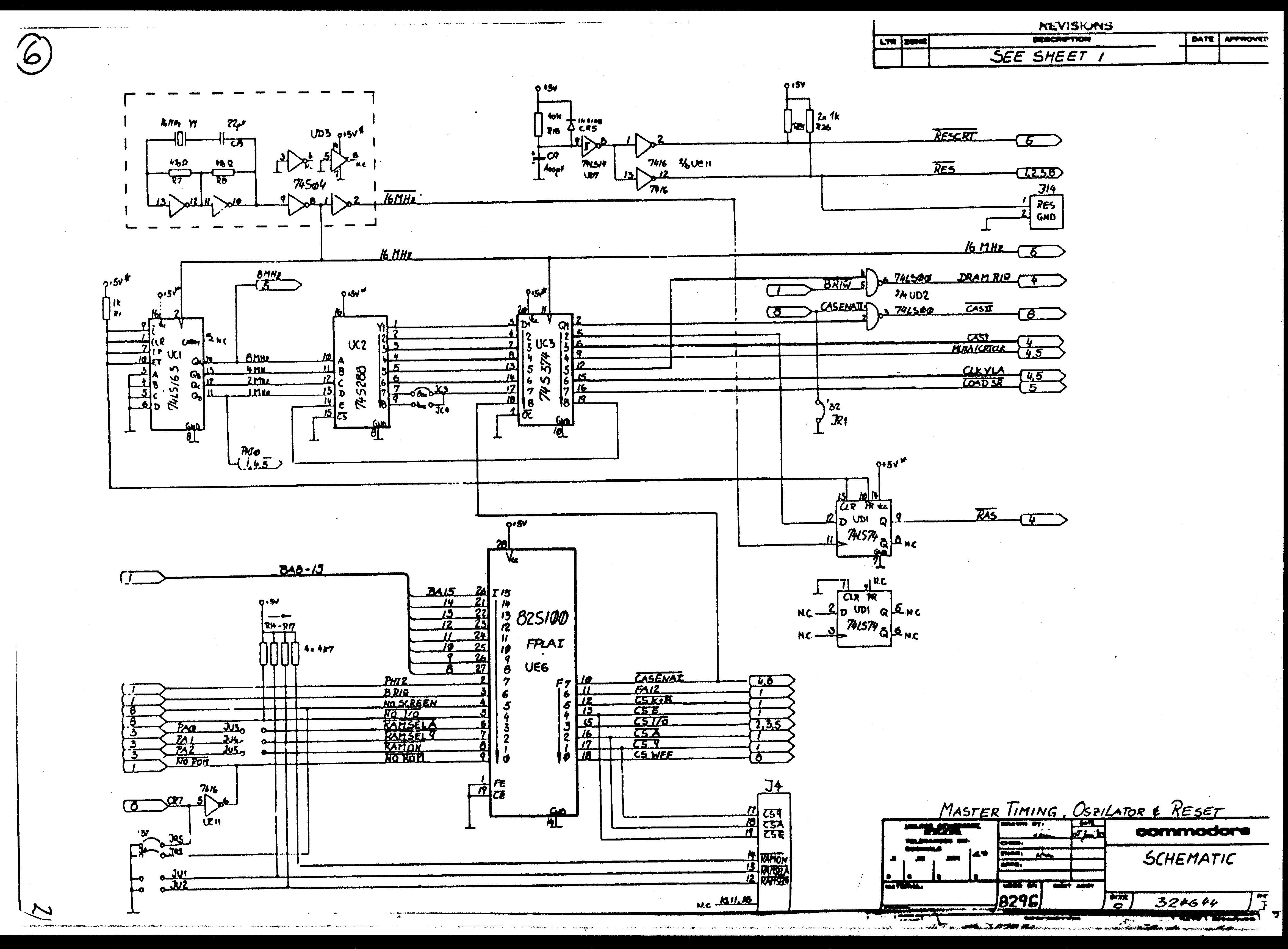
Also, you show a selectable clock rate for the CPU of 8-, 4- and 2MHz. Yet, your expansion connectors only show the 8MHz clock. Logically I would think you would want the same clock that's driving the CPU to be routed to the expansion connectors. Then again, we really don't know how you plan to use this setup and what expansion cards are planned, etc.
Quote:
I would also recommend you ditch the 65C51... any non-WDC parts (sans the xmit bug) will be limited to about 4MHz (if you can find 4MHz rated parts). Going to an NXP SC29L92 DUART would make more sense and give you additional function as well.
Quote:
Finally, have you developed any software for this project yet? Did you do any initial prototyping with some code to make something work so you have an idea on how to get the software side started? Starting with something small at first usually gives you some good insight on how to grow the project.
Re: 65(C)02 Workbench Computer
Ah yes the 6551. I think it has been specially developed to talk to a modem - not like more modern use cases to talk to another rs232 endpoint via null-modem cable. So be aware about the behavior of the handshake lines if you intend to use them. Some work not really as you would expect for a null modem, like interrupting a byte in mid transfer. I'd also recommend another chip. I switched over to the 16550 due to its (potentially past) ubiquity and the fifo buffer - those allow buffering of high speed traffic while waiting for the CPU to serve the interrupt
Author of the GeckOS multitasking operating system, the usb65 stack, designer of the Micro-PET and many more 6502 content: http://6502.org/users/andre/
Re: 65(C)02 Workbench Computer
Regarding clock generation. I was wondering why you use /q of the first register i.e. /4MHz as clock for the second. Not sure if that matters though. Did you draw a timing diagram.
I had a revelation when I saw the timing generator of the Commodore 8296 here left top http://www.zimmers.net/anonftp/pub/cbm/ ... 4-6of9.gif
Using a counter instead of several flip flops, you can use the output directly. Or like in the 8296, slice in a PROM to generate any kind of timing you need from the clock inputs, then qualify with 16MHz so all clocks have the transition at the same time and spurious signals when the PROM input changes do not bleed through
Author of the GeckOS multitasking operating system, the usb65 stack, designer of the Micro-PET and many more 6502 content: http://6502.org/users/andre/
Re: 65(C)02 Workbench Computer
Btw did you check how many unused gates you have? I think I see quite a lot from the layout, although it's difficult to see traces on the back side.
I don't know kicad, but eagle has the tendency if you 'copy' a gate to quietly add a full IC. You have to 'apply' a gate so it shows you unused gates on existing ICs
Also just saw that your schematics also has duplicate inverters for address lines. If you suspect you will need an intermediate signal from one part, better name it and refer to it from another part.
Don't worry it usually takes multiple rounds of refactoring. On more complex boards I usually work multiple weeks with checking, optimizing, re-checking, re-evaluating features in multiple iterations before I get it to production.
Author of the GeckOS multitasking operating system, the usb65 stack, designer of the Micro-PET and many more 6502 content: http://6502.org/users/andre/
- BigDumbDinosaur
- Posts: 9426
- Joined: 28 May 2009
- Location: Midwestern USA (JB Pritzker’s dystopia)
- Contact:
Re: 65(C)02 Workbench Computer
floobydust wrote:
Here's the Rev 2.4 schematic converted to monochrome... hope this is easier to read.
Thanks!
Quote:
I'm not sure why you have so many different ROM banks, but perhaps you can give us some logic on how you plan to use them.
I may have missed it somewhere, but a memory map would be very useful.
Quote:
I would also recommend you ditch the 65C51... any non-WDC parts (sans the xmit bug) will be limited to about 4MHz (if you can find 4MHz rated parts). Going to an NXP SC29L92 DUART would make more sense and give you additional function as well.
Ditto that. The 6551 is very limited compared to other UARTs, even its contemporaries. As André mentioned, the 6551 was intended for use with a modem, not for general-purpose serial communication with another UART. That aspect of its design will needlessly complicate things.
DarkestSoul1992 wrote:
I'm not too sure what version the end user will use (Rockwell most likely?) so I had to try and design that portion around them all. Hence the BE mistake.
At this point in time, designing to accommodate the Rockwell R65C02 is of questionable value, in my opinion. Unlike the Rockwell parts, the WDC 65C02 is in current production and readily available from a number of distributors. Plus it offers a much wider speed range than the Rockwell parts and a fully-static core, a feature that while not of value in a general-purpose computer, is invaluable in debugging a new design with a clock single-stepper.
I absolutely would not even consider an NMOS 6502 as a suitable candidate for any new design.
Quote:
As for the variable clock speed it can be useful to slow programs down and look for errors so I added that for debugging.
You would likely find a clock single-stepper more useful than a variable speed clock for circuit debugging. Most glue logic errors can be drawn out and identified within 18-20 clock cycles after the reset sequence.
Quote:
Quote:
Finally, have you developed any software for this project yet? Did you do any initial prototyping with some code to make something work so you have an idea on how to get the software side started? Starting with something small at first usually gives you some good insight on how to grow the project.
Compiled? Are you writing the firmware in C?
I've not fully examined the schematic, but I believe you have made this too complex for a first effort. The likelihood of it being DOA rapidly increases with complexity. Like Flooby, I recommend you start out with a more basic circuit so you can easily iron out the inevitable bugs. As it stands now, you will be faced with a double whammy: debugging the hardware and debugging the firmware, the latter which you need to debug the hardware. Unless you are an experienced assembly language programmer who has done this sort of thing in the past, there's a likelihood firmware bugs will make it difficult to resolve hardware bugs.
Lastly, please publish a memory map.
x86? We ain't got no x86. We don't NEED no stinking x86!
- GARTHWILSON
- Forum Moderator
- Posts: 8773
- Joined: 30 Aug 2002
- Location: Southern California
- Contact:
Re: 65(C)02 Workbench Computer
DarkestSoul1992 wrote:
I'm not too sure what version the end user will use (Rockwell most likely?) so I had to try and design that portion around them all. Hence the BE mistake.
floobydust wrote:
I would also recommend you ditch the 65C51... any non-WDC parts (sans the xmit bug) will be limited to about 4MHz (if you can find 4MHz rated parts). Going to an NXP SC29L92 DUART would make more sense and give you additional function as well.
Interestingly, BillO has tested several different brands and found that they would all run at several times the rated speed. I don't have any experience with that yet myself, but I have some here to try.
fachat wrote:
Ah yes the 6551. I think it has been specially developed to talk to a modem - not like more modern use cases to talk to another rs232 endpoint via null-modem cable. So be aware about the behavior of the handshake lines if you intend to use them. Some work not really as you would expect for a null modem, like interrupting a byte in mid transfer.
Note that the NMOS 6551 would stop transmission mid-byte if CTS gets taken false mid-byte, whereas the CMOS one (65c51) will finish the byte.
As for not having a FIFO, the fastest it is expected to be used is 115.2kbps, and more typically 19,200 or 9600bps, and with the 6502's excellent interrupt performance, those speeds don't pose any difficulty at all for the '02 to keep up in receiving and keep it busy in transmitting.
Forum member GaBuZoMeu has an elegant solution to the transmit-register-empty-flag bug yet: Use the 51's pin 5 (if in DIP), the x16 clock, as an output to drive a VIA's PB6 for its T2 to count pulses and generate an interrupt. The T2 latch value does not need to change with Φ2 rate nor with baud rate. It's a shame this bug is there; but there is a good solution that does not require software timing loops.
I'm not saying there aren't better UARTs than the '51 of course—there definitely are—but I've been using it for 35 years and have never had any trouble with it, and I used it recently in a work project at 115.2kbps. I have never used the RI pin (ring indicator) since I have not interfaced it to a modem. Another UART I've exercised (but not put to serious use yet) is the 14-pin MAX3100 which is interfaced by SPI.
http://WilsonMinesCo.com/ lots of 6502 resources
The "second front page" is http://wilsonminesco.com/links.html .
What's an additional VIA among friends, anyhow?
The "second front page" is http://wilsonminesco.com/links.html .
What's an additional VIA among friends, anyhow?
- DarkestSoul1992
- Posts: 17
- Joined: 20 Dec 2021
- Location: Glasgow, UK
- Contact:
Re: 65(C)02 Workbench Computer
Quote:
I may have missed it somewhere, but a memory map would be very useful.
Quote:
You would likely find a clock single-stepper more useful than a variable speed clock for circuit debugging. Most glue logic errors can be drawn out and identified within 18-20 clock cycles after the reset sequence.
Quote:
Compiled? Are you writing the firmware in C?
Quote:
I've not fully examined the schematic, but I believe you have made this too complex for a first effort.
Re: 65(C)02 Workbench Computer
Cool! I'm sure you learned a lot!
Can you post the latest version?
Author of the GeckOS multitasking operating system, the usb65 stack, designer of the Micro-PET and many more 6502 content: http://6502.org/users/andre/
- DarkestSoul1992
- Posts: 17
- Joined: 20 Dec 2021
- Location: Glasgow, UK
- Contact:
Re: 65(C)02 Workbench Computer
As requested, the latest version.
- Attachments
-
- Motherboard - Schematic Monochrome.pdf
- monochrome schematic
- (710.66 KiB) Downloaded 57 times
-
- Motherboard - Schematic Colour.pdf
- colour schematic
- (725.83 KiB) Downloaded 50 times
Re: 65(C)02 Workbench Computer
If you want to save more chips I think you can combine some of the 138... u3 and u9 have the same inputs, same with u4 and u8.
Author of the GeckOS multitasking operating system, the usb65 stack, designer of the Micro-PET and many more 6502 content: http://6502.org/users/andre/
- floobydust
- Posts: 1394
- Joined: 05 Mar 2013
Re: 65(C)02 Workbench Computer
Having examined your latest schematic (2.5), you should take a closer look at your I/O decode and chip selects for the various I/O devices.
You're using a pair of 74HCT138 chips to decode an I/O page of $D000, where the first one decodes the upper 4-bits to a "D" and the second one decodes the lower 4-bits to a "0". This works, but the outputs from the 74HCT138 decoders are active low. You're using a single 74HCT08 AND gate to obtain an active high signal for CS_DEV. This doesn't work as the AND gate requires both inputs to be active high to obtain an active high output. As you have multiple inverters leftover from the 74HCT04, you could use two of those to invert the output signals from the 74HCT138s driving the AND gate. This will result is a longer delay path due to the additional chips in the circuit.
Looking at the 65C22 used for GPIO, you have the CS1 and /CS2 lines reversed, i.e., the CS_DEV (which should be active high, goes to /CS2 and the CS_GPIO (which is active low) goes to CS1.
U4 and U10 are wired the same on input (as previously noted). The output selects start at $xx80 and increase by $xx10 to $xxF0. Note that $xx is $D0 based on CS_DEV.
- You show the UART I/O as $D014 - $D017, but the base select is $D090
- You show the 65SIB I/O as $D0C0 - $D0CF, but the base select is $D0A0
Regards, KM
https://github.com/floobydust
- DarkestSoul1992
- Posts: 17
- Joined: 20 Dec 2021
- Location: Glasgow, UK
- Contact:
Re: 65(C)02 Workbench Computer
Many thanks for all the help from everyone and any pointers/constructive criticisms. I have had a lot of ideas and help from you all.
Thanks floobydust, I noticed these issues too after I triple checked all the address decoding. This has been changed in the repository but I forgot to repost the schematics here. (Sorry everyone.) Changed the inputs and outputs on the 138s to reflect their true addresses and changed the CS_DEV AND gate to a NOR so that it goes HIGH when both signals are LOW. I believe the AND was left there from when the CS_DEV line was active LOW. Just goes to show that I shouldn't work without sleep.
Quote:
Having examined your latest schematic (2.5), you should take a closer look at your I/O decode and chip selects for the various I/O devices.
Re: 65(C)02 Workbench Computer
U9 has two outputs that are combined with an AND. you can achieve the same result by removing A13 from the input, setting the input to low and then use the 138 output directly.
That leads to the question where A13 feeds into address selection. If I get it right A13 is not used, so you have 8k ROM pages, that are mirrored two times into a 16 address space.
Last edited by fachat on Wed May 11, 2022 8:48 pm, edited 1 time in total.
Author of the GeckOS multitasking operating system, the usb65 stack, designer of the Micro-PET and many more 6502 content: http://6502.org/users/andre/
Re: 65(C)02 Workbench Computer
Regarding the findings from floobydust, it helps to note the type of logic in the signal name. For example mark active low signals with a '/' prefix, or a N prefix or postfix. WDC notes them with a B postfix IIRC.
This way when you change the logic you either create separate signals and electrical rule check should warn you that a signal has no output, or if you rename a signal you can see the changed logic in the other places where it's used
Author of the GeckOS multitasking operating system, the usb65 stack, designer of the Micro-PET and many more 6502 content: http://6502.org/users/andre/
Re: 65(C)02 Workbench Computer
since you're using Kicad you can also just name your active low labels/signals ~{name} which will put a negation line above them
also personally i always start by making my decoding circuit in a logic simulator to see if it even works, what gates it needs, and what could be optimized away.
especially when you're using discrete logic gates instead of something programmable, where mistakes are a bit more resilient.
also personally i always start by making my decoding circuit in a logic simulator to see if it even works, what gates it needs, and what could be optimized away.
especially when you're using discrete logic gates instead of something programmable, where mistakes are a bit more resilient.