
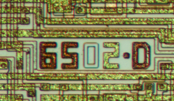
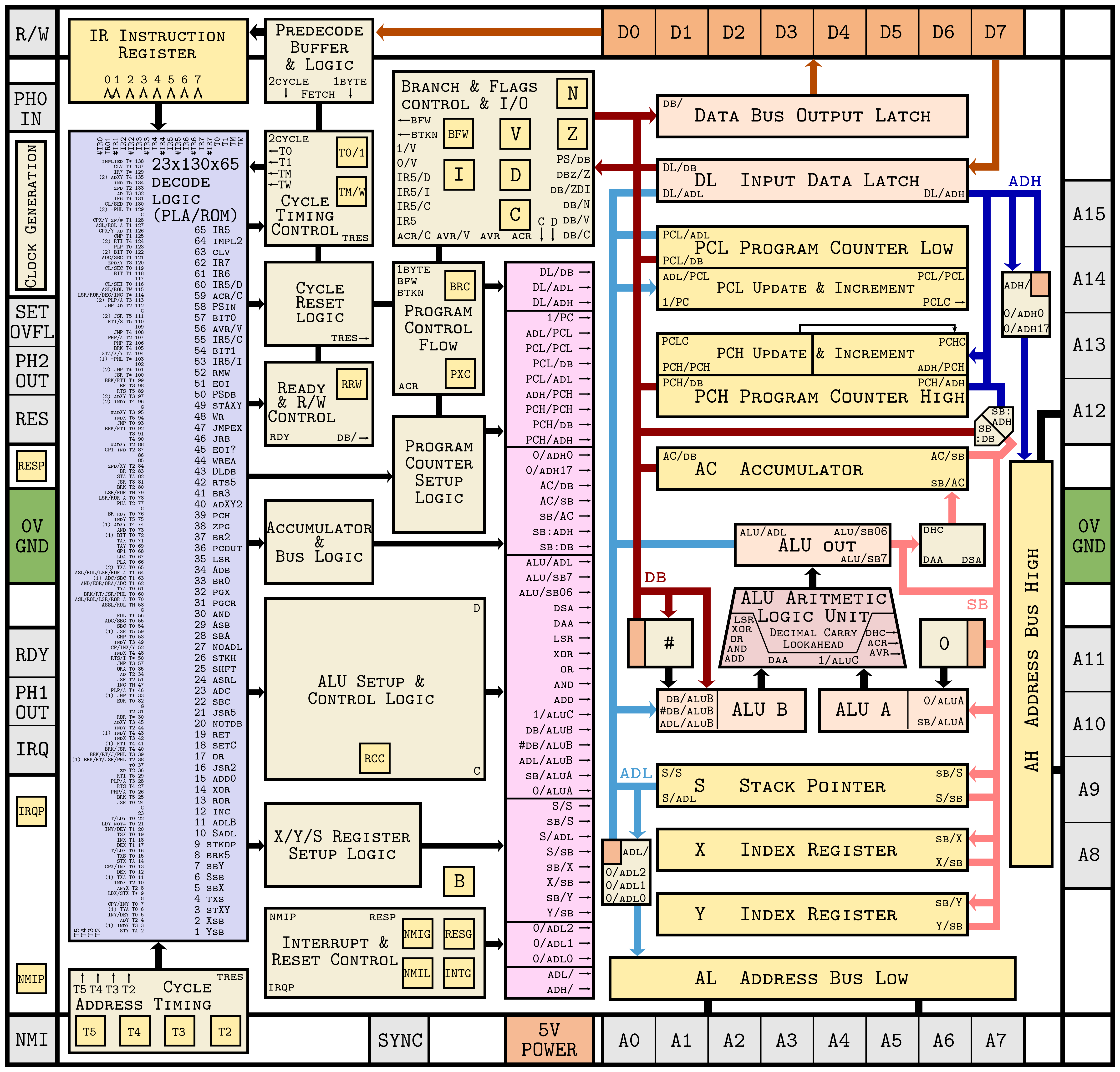
I created an svg circuit diagram of the 6502 which is now available (in a first draft) at https://davidmjc.github.io/6502/cd.svg. This is based primarily on the circuit diagram by Balazs Beregnyei (of which it is a derivative work, by permission) but I also made use of BreakNES and the Visual 6502. Although I don't think it qualifies as a derivative work of either of the latter, I chose the license cc-by-sa for maximum compatibility.
Disclaimer: this is not a 100% faithful representation of the 6502 circuit. I fell into this project in stages and made several questionable design decisions along the way. In particular, my goal was not fidelity, but understanding. My initial motivation was to understand the instruction decode of the 6502 as a fully fledged PLA, with both an AND and an OR plane (implemented as NOR-NOR in nmos logic): indeed a large part of the so-called "random logic" of the 6502 can be viewed as a space-optimized OR plane. However, to bring this out, I reordered a few PLA lines, and moved timing control lines for the read-modify-write cycle (which I call TA, TM and TW) into the PLA. This reduces the random logic considerably, and makes it easier (for me at least) to understand.
I have tried to lay out the circuit much like the original chip (with Hanson orientation, i.e., PLA on the left, data path on the right) but circuit diagrams and silicon chips have somewhat different constraints, so many compromises were necessary. Nevertheless I found the iconic layout of the 6502 quite inspirational for drawing this circuit diagram. My diagram likely contains many errors, as I found many along the process of creating it. Some of these errors are deliberate (e.g. using the same circuit for both halves of the decimal half carry which the 6502 does not). However, modulo these issues, I would like to think my diagram is still 99.9% faithful to the original 6502 circuit, and maybe 95% like the original layout!
One of my main motivations for releasing it under a free license is so that other 6502 enthusiasts can go back and fix my errors and dubious design decisions (e.g., by producing a completely faithful representation of the original 6502). I would be happy to be more specific about changes I made to anyone interested (although sadly I did not keep notes - my biggest regret).
The svg has some interactivity in a suitable browser (you can mouse-over or click on nmos circuits), but this is not completely developed in this draft. I would welcome comments and suggestions for features to add (or links to your own additions based on this freely licensed work!).
6502 svg schematic

Re: 6502 svg schematic
Very welcome, thank you for contributing this to the commons!
(About orientation: I remember being disturbed by the visual6502's choice when I first saw it. But I think it is the orientation of the chip in the package, and of the blueprints rescued by Donald Hanson. Hanson's block diagram is rotated, Balazs' is upside down, and there's another set - is it Atari's? - which is the same as Balazs'. One must take what one is given!)
(About orientation: I remember being disturbed by the visual6502's choice when I first saw it. But I think it is the orientation of the chip in the package, and of the blueprints rescued by Donald Hanson. Hanson's block diagram is rotated, Balazs' is upside down, and there's another set - is it Atari's? - which is the same as Balazs'. One must take what one is given!)
Re: 6502 svg schematic
Surely the right way up is whichever way puts this bit the right way up:
...which in this case is PLA at the top.
...which in this case is PLA at the top.
Re: 6502 svg schematic
I have a live and let live attitude to orientations (in general!). One advantage of a freely licensed diagram is that anyone is welcome to download it, rotate it and release their preferred version under cc-by-sa! I did most of my editing of the svg with the Balazs orientation, so it was a bit of a jolt for me when I switched to Hanson. My main motivation for making the change was that I had previously produced my own version of the block diagram (which I have now added as an svg and png to davidmjc/6502: the png is https://davidmjc.github.io/6502/bd.png) and I would like at some point to combine the two. Having a vertical data path is quite convenient in a block diagram, because the bit slices are horizontal, making it easier to label the registers. But as I say, each to his/her/zir own!
Now can we have a debate about whether the 6502 uses microcode
Now can we have a debate about whether the 6502 uses microcode
Davidmjc
Re: 6502 svg schematic
That's certainly a nice block diagram!
Re: 6502 svg schematic
Thanks - I did this mostly in 2018, so it is not up to date with respect of my current understanding of the chip. For instance, I now find the "Data output register" to be something of a chimera! I did at least rename "RESB" to "BRC" (for branch carry) as I believe this circuit is more about timing control on branches than reset logic. Is there any history behind names such as these?
Davidmjc
Re: 6502 svg schematic
I think there are several sources for internal signal names - Hanson's block diagram takes names from the giant MOS schematics. There are names on the Atari schematics. Some names predate visual6502 - either from Balazs or other independent investigations - and some names were conjured up by visual6502. The visual6502 wiki may provide some hints.
Re: 6502 svg schematic
As suggested above, I have now produced a version of the circuit diagram with a block diagram overlay. In a suitable browser the overlay can be switched off (or on again) by clicking on the title. It can be found at https://davidmjc.github.io/6502/bcd.svg.
Any suggestions for other improvements/bells-and-whistles are welcome!
Any suggestions for other improvements/bells-and-whistles are welcome!
Davidmjc
Re: 6502 svg schematic
Very nice indeed! Here's a screenshot:
Re: 6502 svg schematic
Thanks. Note that in the screenshot, the fonts have not been rendered correctly (this is probably a browser-dependent issue). Also you can click on the black squares next to the title to get more text detail (not a great user interface at present, I admit!).
Davidmjc
Re: 6502 svg schematic
Wow - thanks for the tip on the black squares. I think that makes for 4 different views of the various layers. There really is a lot of annotation here - and tooltips too, and highlighting of nets.
I've added a github issue for a few things I've noticed.
I've added a github issue for a few things I've noticed.
Re: 6502 svg schematic
Thanks. I made those fixes. It looks like the font issue is not about the browser, but whether the font is installed by the OS. The font in question is Latin Modern Mono Caps. I could include the font specification in the svg or convert the text to paths, but both solutions would increase the size of the svg, which I have been trying to keep small. A perhaps nicer solution would be to get the browser to download the font from the internet, but I haven't figured out how to do this.
Concerning features, it would be easy enough to add buttons to switch other layers off or on, but maybe it would get a bit complicated (unless it was just in an "advanced" mode a la visual 6502!).
Concerning features, it would be easy enough to add buttons to switch other layers off or on, but maybe it would get a bit complicated (unless it was just in an "advanced" mode a la visual 6502!).
Davidmjc
Re: 6502 svg schematic
Thanks for the fixes!
Looks like perhaps 'Courier' would work everywhere, or perhaps you can figure out Web Fonts - that's what this page seems to suggest:
https://vecta.io/blog/using-fonts-in-svg
Looks like perhaps 'Courier' would work everywhere, or perhaps you can figure out Web Fonts - that's what this page seems to suggest:
https://vecta.io/blog/using-fonts-in-svg
Re: 6502 svg schematic
I haven't had any luck figuring out how to use web fonts or embedded fonts. I've added Courier as a back-up font for the annotation layers, but it is too big to use as a substitute font in the block diagram layers, so I've used Consolas instead, which at least works on my Windows 10 system. There doesn't appear to be a decent portable small caps font.
I find the way the web handles fonts to be baroque to say the least, and I probably don't have the patience to resize all the text to get it to work with a less satisfactory font! If someone else wants to have a go at making a nice portable version, be my guest...!
I find the way the web handles fonts to be baroque to say the least, and I probably don't have the patience to resize all the text to get it to work with a less satisfactory font! If someone else wants to have a go at making a nice portable version, be my guest...!
Davidmjc
-
randallmeyer2000
- Posts: 255
- Joined: 12 Oct 2015
Re: 6502 svg schematic
Those of you who have followed my sporadic posts know my interest in 6502 schematics.
How do I turn a NMOS original 6502 schematic into a two color. laser computer, using only laser pointers and dichroic mirrors? FOICs for "wires". Fiber Optic Image Couplers.
I will continue to consider the analogy of "path decision" mirrors, based on "color discrimination" logic, to the original enhancement and depletion mode, NMOS transistors.
But does this help in any way? Fiber optics can't get nanometer small?
Light travels slower in glass than in vacuum or air and probably slower than electrons in a wire ( velocity factor : ladder line or twisted pair seem to be fastest?).
The largest CPU, commercial, to date, is an (Apple/TMSC?) Max 1, I think? With something like 59 billion transistors.
Let's try to get a 50/50 duty cycle , Pico or femtosecond laser, (500 GHz or 1 THz clock?), and , at about 4,500 transistors per core, build a 12,600,000 core 6502 multiheaded hydra ?
Nuts you say? Maybe? Maybe it would be desk sized, not chip sized. But it would be NEAT !!!!
We can make a bit coin rig and mine all the bitcoin that is left in a year or two instead of the projected 20 or so years?
Then buy all the real money in the world with it. And relax and. retire to Cancun or the virgin islands.
Yes. St Thomas maybe? Go visit Lillienfeld's old house?