6502.org Forum  Projects  Code  Documents  Tools  Forum
It is currently Fri Sep 27, 2024 7:33 am

All times are UTC


Post new topic Reply to topic  [ 91 posts ]  Go to page Previous  1 ... 3, 4, 5, 6, 7  Next
Author Message
PostPosted: Wed Apr 22, 2020 12:48 pm 
Offline
User avatar

Joined: Wed Apr 22, 2020 7:17 am
Posts: 6
Location: Madrid, Spain
Quote:
I might be missing the point of what you're trying to achieve here. It sounds overly complicated compared to using an external tristate buffer and doing DMA during Phi1.

I am proposing a solution to the lead post in this thread.

The point is that the datasheet does not assure we can avoid data bus contention with the timing specs it gives. And memory can write to the data bus when the CPU is still driving the bank address in the lines.

Using a tristate buffer just moves the problem around. Because you will still have a data bus (the one that goes from the CPU to whatever you put there: transceiver, buffer, etc) and two devices writing to them at once.


Top
 Profile  
Reply with quote  
PostPosted: Wed Apr 22, 2020 2:11 pm 
Offline

Joined: Mon May 21, 2018 8:09 pm
Posts: 1462
Hmm, I see now. But you also have to remember that BE takes time to activate and deactivate. The datasheet says 25ns, which is comparable to the data access time, and much longer than the hold times of the relevant signals. So you can't rely on it to get the CPU off the bus sooner than it ordinarily would at high speed. An external buffer may react faster.

But the tristate outputs of a typical SRAM also take time to switch on and off. It just so happens that the basic 55ns Alliance devices specify a minimum 10ns before they go low-Z, and a maximum 30ns before the output is stable and valid - which matches perfectly with the WDC datasheet. Of course, other devices will vary.


Top
 Profile  
Reply with quote  
PostPosted: Wed Apr 22, 2020 2:33 pm 
Offline
User avatar

Joined: Wed Apr 22, 2020 7:17 am
Posts: 6
Location: Madrid, Spain
Oh, nice catch! Yes, tBVD (be TO Valid Data) max is 25ns. This makes my proposal unfeasible.

Many thanks for the info!


Top
 Profile  
Reply with quote  
PostPosted: Wed Apr 22, 2020 3:40 pm 
Offline
User avatar

Joined: Thu Dec 11, 2008 1:28 pm
Posts: 10938
Location: England
It was an interesting idea...

Might be worth noting that it's difficult to characterise the time to Z, so datasheets often have a disclaimer, that it's typical. Sometimes you'll see a test circuit - essentially you have to have an opposing driver or pullup in order to see that the device under test has stopped driving.


Top
 Profile  
Reply with quote  
PostPosted: Wed Apr 22, 2020 4:14 pm 
Offline
User avatar

Joined: Wed Apr 22, 2020 7:17 am
Posts: 6
Location: Madrid, Spain
However, I think the idea of the three shifted clock signals is promising. Even though not using BE signal at all.

Let's have a look to the following timing diagram:

Attachment:
weena-timings.png
weena-timings.png [ 39.33 KiB | Viewed 3066 times ]


In the top block we have the three clock signals shifted 10ns each other. Please note I am using 12Mhz frecuency here, although we will use the 14Mhz AC requirements. After clocks, we have the relevant CPU signals, the memory bus signals and the SRAM chip.

I used the following time marks to point out significant events:

  • A: PHI2 raise edge. This is the strobe signal for address and bank address. The memory controller latches the bank address in a register. And MA (Memory Address) is driven with the 24 bits of the address obtained from A and D.
  • B: 10ns after PHI2 raise edge. The MAS (Memory Address Strobe) signal is asserted. This will be used by the selected SRAM chip to read (specific chip selection by address range is not included in the diagram).
  • C: the SRAM chip responds to the read and drives the memory data bus. This is not the same bus as the CPU data bus. They are separated. Thanks to this, we are not in risk of bus contention at this point. The SRAM chip can be as fast as possible. An access time of 0 would be acceptable.
  • D: 10ns before PHI2 fall edge. The memory controller activates the buffer that drives the CPU data bus from the Memory data bus. This causes the data read from the memory to be accessible by the CPU. Please note this is 10ns before the CPU reads the byte. It is almost impossible that it is still driving the bus for BA.
  • E: PHI2 fall edge. The CPU reads the data from its data bus.
  • F: 10ns after PHI2 fall edge. The memory controller stops driving the CPU data bus and it deactivates the MAS signal. Please note this is 10ns after CPU reads the byte. It is almost impossible that it is writing BA for the next access so soon.

So yes, the circuit is more complicated. Not much for a CPLD. But thanks to this we can be confident the memory will not cause bus contention, even if it has an access time of zero.

How does it look?


Top
 Profile  
Reply with quote  
PostPosted: Wed Apr 22, 2020 4:37 pm 
Offline
User avatar

Joined: Fri Dec 11, 2009 3:50 pm
Posts: 3367
Location: Ontario, Canada
apoloval wrote:
I am proposing a solution to the lead post in this thread.
Welcome,apoloval, and thanks for your interest. :)

apoloval wrote:
Yep, my fault. I said RDY, but I meant BE (Bus Enable).
Ummmm.. is it possible you subsequently made another mistake expressing yourself? I think I know what you mean, but it seems to differ from what you said. :|

Here is a portion of the diagram I included in the lead post. I added some stuff pertaining to your suggestion, and the notations at the bottom are direct quotes taken from your post. As I write this I see you have posted again, but I'll finish what I was saying for the sake of anyone else who (like me) was confused.
Attachment:
'816 bus activity 01.png
'816 bus activity 01.png [ 6.62 KiB | Viewed 3064 times ]

That makes no sense to me (look what BE is doing), so I wondered if you had two inverters separating the A, B and C clock signals. But that makes no sense either:
Attachment:
'816 bus activity 02.png
'816 bus activity 02.png [ 6.72 KiB | Viewed 3064 times ]


Here (below) is what I think you meant. And it results in BE dropping low briefly during one of the hazard points. I like the idea, but it has some challenges. Also, it offers no remedy for the other hazard point .
Attachment:
'816 bus activity 04.png
'816 bus activity 04.png [ 6.74 KiB | Viewed 3064 times ]


I look forward to reading your latest post. For bonus points, it'd be nice if it takes account of the fact that the data bus has to be passed both back and forth, so to speak. In other words, there are two "sticky wickets" in the transaction.

cheers,
Jeff

_________________
In 1988 my 65C02 got six new registers and 44 new full-speed instructions!
https://laughtonelectronics.com/Arcana/ ... mmary.html


Top
 Profile  
Reply with quote  
PostPosted: Wed Apr 22, 2020 5:20 pm 
Offline
User avatar

Joined: Thu May 28, 2009 9:46 pm
Posts: 8402
Location: Midwestern USA
— deleted —

_________________
x86?  We ain't got no x86.  We don't NEED no stinking x86!


Last edited by BigDumbDinosaur on Thu Apr 23, 2020 1:20 am, edited 2 times in total.

Top
 Profile  
Reply with quote  
PostPosted: Wed Apr 22, 2020 5:29 pm 
Offline
User avatar

Joined: Fri Dec 11, 2009 3:50 pm
Posts: 3367
Location: Ontario, Canada
BigDumbDinosaur wrote:
Comments?
No offense, but I don't see how this furthers the discussion... which, to me, seems very much in danger of going off into the weeds because (IMO) of people being too hasty. apoloval seemingly made two erroneous posts in a row, then quickly changed tacks. Myself, I'd prefer to tie up some loose ends before proceeding.

_________________
In 1988 my 65C02 got six new registers and 44 new full-speed instructions!
https://laughtonelectronics.com/Arcana/ ... mmary.html


Top
 Profile  
Reply with quote  
PostPosted: Thu Apr 23, 2020 1:20 am 
Offline
User avatar

Joined: Thu May 28, 2009 9:46 pm
Posts: 8402
Location: Midwestern USA
Dr Jefyll wrote:
BigDumbDinosaur wrote:
Comments?
No offense, but I don't see how this furthers the discussion... which, to me, seems very much in danger of going off into the weeds because (IMO) of people being too hasty. apoloval seemingly made two erroneous posts in a row, then quickly changed tacks. Myself, I'd prefer to tie up some loose ends before proceeding.

That's why I said "comments." I wasn't sure if I was contributing or muddying the waters. Ignore my post.

_________________
x86?  We ain't got no x86.  We don't NEED no stinking x86!


Top
 Profile  
Reply with quote  
PostPosted: Thu Apr 23, 2020 3:34 am 
Offline
User avatar

Joined: Fri Dec 11, 2009 3:50 pm
Posts: 3367
Location: Ontario, Canada
Hello again, all, and sorry for the delay. (And no worries, BDD.) apoloval, does the correction I offered regarding your BE post seem appropriate? I get that you want to avoid bus contention during the time of the first hazard (roughly when Phi2 rises) by forcing one of the contending parties to desist. (By parties I mean the '816 CPU and whatever device is attached to it on the motherboard.)

Your most recent post describes a more familiar and more effective setup. Instead of controlling the CPU's BE you're controlling a transceiver aka tristate buffer that separates the CPU data bus and the memory data bus. ( Separate data buses linked by a transceiver is a typical configuration, suggested in the WDC '816 datasheet. )

I'll begin by reviewing the second half of the cycle. This is the handoff from the CPU to the buffer. The buffer (which will be delivering read data) remains disabled until...
Quote:
  • D: 10ns before PHI2 fall edge. The memory controller activates the buffer that drives the CPU data bus from the Memory data bus. [...]
  • E: PHI2 fall edge. The CPU reads the data from its data bus.
Alright, that makes sense, but what allows you to drive the data bus at exactly the time you mention? In real life, the buffer takes some inexactly known amount of time to begin driving. Rather than giving an exact figure, the datasheet for the buffer states the minimum and maximum enable time (the time from when the buffer is told to begin driving until it actually does so).

For ease of discussion, let's say the buffer-enable delay is listed as min 0 to max 5 ns. And in the diagram below, tDSR from the '816 datasheet tells us the deadline by which the read data needs to be valid -- there needs to be at least 10 ns of setup time before Phi2 falls. Assuming, as I said, between zero and 5 ns of buffer-enable delay, that means for reliable operation the buffer needs to be told to enable 15 ns before Phi2 falls.

Trouble is, we have no explicit assurance the CPU will have stopped driving by then. :(
Attachment:
File comment: 
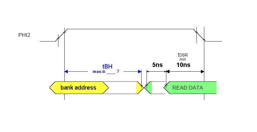
handoff from the CPU to the transceiver
65816 timing01.png
65816 timing01.png [ 6.44 KiB | Viewed 2972 times ]
Because we know how long the Phi2-high pulse lasts, all it takes is some simple math to reveal what's the largest tBH figure we can tolerate. But the '816 datasheet fails to specify a max figure for tBH; only a min figure appears. As far as I can tell, the omission of a max tBH figure scuttles any attempt at a rigorous solution for avoiding contention. WDC's omission forces us to use seat of the pants solutions rather than real engineering. :!:

( I can think of factors that lessen the bad news about contention, and I can think of factors that make it worse. But for the moment let me stay on focus. And to be clear: I'm not saying seat of the pants solutions are ineffective -- I'm just saying we shouldn't be forced to work that way. )


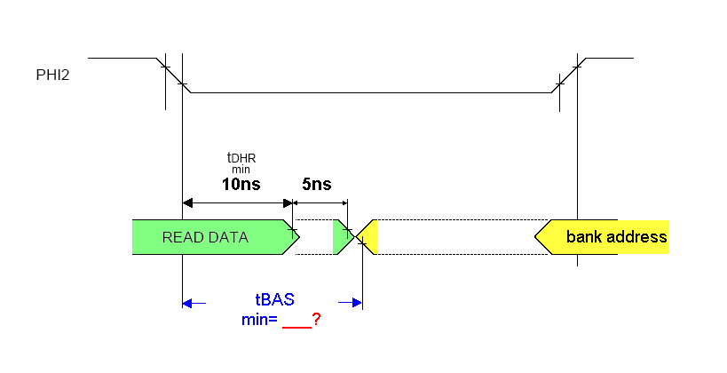
Now here's the other handoff, this one from the buffer to the CPU. It's a similar situation, unfortunately.
Attachment:
File comment: handoff from the transceiver to the CPU
65816 timing02.png
65816 timing02.png [ 6.2 KiB | Viewed 2972 times ]

The '816 datasheet tells us data on the bus must remain valid for at least 10 ns after the fall of Phi2 -- this is tDHR -- and let's assume the buffer has a 0 to 5 ns disable delay. If the buffer is told to disable 10 ns after the fall of Phi2 then in total it may drive as late as 15 ns past the fall of Phi2.

Now we have a figure (15 ns) for the smallest tBAS figure we can tolerate before a collision occurs. We don't want the Bank Address to appear too soon. But the '816 datasheet doesn't offer any warning or reassurance about the possibility of tBAS being smaller than 15 ns. No min figure for tBAS is specified; only a max figure is provided!! :roll:

I think we all realize bus capacitance can usually be relied upon to maintain the state of the bus for a short time, and thus the command to disable the buffer needn't be as late as I suggested (ie, it can be earlier than 10 ns after the fall of Phi2). But you mustn't disable it too early or it'll fail to establish valid levels in the first place.

Instead I wish WDC had simply provided a min figure for tBAS and a max figure for tBH as they ought to have done -- that's what I'm mainly saying.


apoloval wrote:
  • A: PHI2 raise edge. This is the strobe signal for address and bank address. The memory controller latches the bank address in a register. And MA (Memory Address) is driven with the 24 bits of the address obtained from A and D.
  • B: 10ns after PHI2 raise edge. The MAS (Memory Address Strobe) signal is asserted. This will be used by the selected SRAM chip to read (specific chip selection by address range is not included in the diagram).
There's maybe something you're missing here, which I'll deal with quickly as it doesn't affect what I had to say above. It's necessary for the system to acquire the entire 24-bit address before Phi2 rises. That's so there'll be enough time for the memory decoder to select the appropriate RAM, ROM, or peripheral. Note that 65xx peripherals such as the 65C22 VIA require their chip-select inputs to be valid before Phi2 rises. Although it may be said that the Bank Address "is latched" when Phi2 rises, remember it's a transparent latch that's presumed -- ie, a '573, not a '574. Thus the Bank Address will already be flowing through the latch before Phi2 rises. When Phi2 rises it then stops flowing, freezing the state established before.

Hoping all that's clear... whew! :)

Jeff
[edit: better diagrams, tweaked text]

_________________
In 1988 my 65C02 got six new registers and 44 new full-speed instructions!
https://laughtonelectronics.com/Arcana/ ... mmary.html


Last edited by Dr Jefyll on Sat Apr 25, 2020 2:30 am, edited 1 time in total.

Top
 Profile  
Reply with quote  
PostPosted: Thu Apr 23, 2020 8:41 am 
Offline
User avatar

Joined: Wed Apr 22, 2020 7:17 am
Posts: 6
Location: Madrid, Spain
Quote:
Ummmm.. is it possible you subsequently made another mistake expressing yourself? I think I know what you mean, but it seems to differ from what you said. :|

Quote:
No offense, but I don't see how this furthers the discussion... which, to me, seems very much in danger of going off into the weeds because (IMO) of people being too hasty. apoloval seemingly made two erroneous posts in a row, then quickly changed tacks. Myself, I'd prefer to tie up some loose ends before proceeding.

Absolutely agree. I make mistakes expressing myself, and I am too hasty. Mainly because of three reasons.

  1. English is not my mother tongue.
  2. I didn't really mean to document a working solution. But mainly give new ideas and think aloud. That's why I am not going deeper in many details, assuming we all can focus on the general idea. For example, I didn't explain the 7404 must be used such as inverters are connected by pairs. I just assumed it was obvious for the reader considering I said the clock signals where shifted in time.
  3. Being isolated by COVID with 2-yo kids makes you optimise your time to the maximum. Each second of spare time is gold. That's why I said RDY without double checking it was actually BE.

Quote:
apoloval, does the correction I offered regarding your BE post seem appropriate?

Yes, absolutely. I was assuming we could generate a BE negative pulse also for the falling edge of PHI2. But I am not sure, and I don't think this is documented anywhere, that the CPU can read from the bus when BE is inactive. However, what convinced me that this is not a safe way is the propagation delay of BE: max 25ns is extremely high.

Quote:
Instead I wish WDC had simply provided a min figure for tBAS and a max figure for tBH as they ought to have done -- that's what I'm mainly saying.

Yes, totally agree. In fact, this is how I reached this forum topic. I read the timing diagrams and the requirements from the WDC datasheet, and they are totally insane. Google has this thread and your initial figure indexed when you search for "65c816 tBH min". I think anyone who wants to implement a memory management circuit reaches the same conclusion.

However, we have two alternatives. We can ignore 65816 CPU and use better documented parts in our designs. Or we can figure out how to minimise the risk of bus contention. My goal is the latter.

About my design and its drawbacks. Yes, I know the transceiver will have its own enable propagation delays. However, my plans are to use a CPLD to implement the memory management logic. I am totally newbie in the CPLD world and I could be mistaken, but I think the propagation delays inside the CPLD are rather low (below 1ns). At this moment, my main concern is how to generate the three clock signals with an accurate shift. Because, again, the 7404 datasheets do not ensure a minimum propagation delay, but just a maximum.

Anyway, many thanks Jeff for your replies and the very detailed explanations. They are really useful!

Also many thanks BigDumbDinosaur for the data you shared. IMO, they are really useful. I might be totally wrong on this, but I figure out this is how the timing requirements are documented in the datasheets. The manufacturer perform experiments in the laboratory under controlled conditions (voltage, capacitance, temperature, humidity, etc). And they take note on the maximum or minimum delays of their parts. And how they respond to certain changing parameters such as temperature or voltage to document curves in their datasheets.

Yes, I know. The manufacturer likely uses hundreds of units for these measurements, and you had only used once. And their conditions are controlled while yours likely aren't. But this is better than nothing. At least we have some reference typical values, even though the confidence level is not high.


Top
 Profile  
Reply with quote  
PostPosted: Thu Apr 23, 2020 9:30 am 
Offline
User avatar

Joined: Thu Dec 11, 2008 1:28 pm
Posts: 10938
Location: England
It's a recurring theme that WDC's offering, especially their documentation, falls short of best practice.

It's even possible that there's no bus contention, if the various underspecified and misdocumented parameters work out the right way.

Perhaps the best way to test is by tracing voltages dropped by some 1 ohm resistors strategically placed in line.

Which leads to another thought: some low resistances inline with the signals of interest will dissipate some of the energy wasted by contention. And another thought again: how much energy are we talking about? How much damage or temperature rise is anticipated by very brief overlaps of opposite-sense driving?


Top
 Profile  
Reply with quote  
PostPosted: Thu Apr 23, 2020 9:50 am 
Offline
User avatar

Joined: Wed Feb 14, 2018 2:33 pm
Posts: 1467
Location: Scotland
BigEd wrote:
It's a recurring theme that WDC's offering, especially their documentation, falls short of best practice.

It's even possible that there's no bus contention, if the various underspecified and misdocumented parameters work out the right way.

Perhaps the best way to test is by tracing voltages dropped by some 1 ohm resistors strategically placed in line.

Which leads to another thought: some low resistances inline with the signals of interest will dissipate some of the energy wasted by contention. And another thought again: how much energy are we talking about? How much damage or temperature rise is anticipated by very brief overlaps of opposite-sense driving?


We're probably veering off a a tangent to the original posting here, but perhaps (and maybe for the benefit of apoloval and others finding this thread?) it's worth noting that now, in 2020, we have many people here and elsewhere who have developed successful '816 systems and while they may well have a few nanoseconds of contention on the data bus, these systems do work.

Commercial systems include the Apple //gs, SNES and the Acorn communicator - these were all made back in the 1980's and while relatively low clock speeds (< 4Mhz?) I'm sure any hardware issues in these would be well known and documented by now.

Today there are 2 (to my knowledge) commercial '816 systems that you can buy - the Foenix and Neon816 as well as many hobby systems here and elsewhere. My own 65816 board uses a single GAL and no bus transceiver and runs at 16Mhz. Nothing is getting hot, current consumption is about what I'd expect (and it's the GALs getting marginally above ambient temperature and not the WDC or memory parts) Others here are using the data-sheet latch and buffer solution and others are using a CPLD, so bringing up an '816 system doesn't appear to be as hard as it might have been made-out at a first glance of the datasheets...

So I do wonder that if, by-now it's really moot.

And, apoloval, if you are thinking of making a 65816 system, then just do it - don't overthink it, just enjoy the process!

Cheers,

-Gordon

_________________
--
Gordon Henderson.
See my Ruby 6502 and 65816 SBC projects here: https://projects.drogon.net/ruby/


Top
 Profile  
Reply with quote  
PostPosted: Thu Apr 23, 2020 9:53 am 
Offline
User avatar

Joined: Thu Dec 11, 2008 1:28 pm
Posts: 10938
Location: England
(It might be good to have a new thread with a head post that catalogues 816 designs, with links where possible?)


Top
 Profile  
Reply with quote  
PostPosted: Thu Apr 23, 2020 11:25 am 
Offline

Joined: Mon May 21, 2018 8:09 pm
Posts: 1462
Also worth remembering the inherent characteristic of CMOS, which is that both transistors in the totem pole are briefly switched on simultaneously during their input's transition. CMOS remains power efficient because that "shoot-through" period is extremely brief, but it does mean there is a measurable current spike in the vicinity of clock edges - which is in part why power plane decoupling is needed.

I would suggest that any temporary contention during bus turnaround is indistinguishable from the inherent shoot-through of the driving circuits.


Top
 Profile  
Reply with quote  
Display posts from previous:  Sort by  
Post new topic Reply to topic  [ 91 posts ]  Go to page Previous  1 ... 3, 4, 5, 6, 7  Next

All times are UTC


Who is online

Users browsing this forum: No registered users and 26 guests


You cannot post new topics in this forum
You cannot reply to topics in this forum
You cannot edit your posts in this forum
You cannot delete your posts in this forum
You cannot post attachments in this forum

Search for:
Jump to: