are ceramic 0.1uF caps enough for decoupling capacitors? or is there another type i should be using?
I'll just assume every unpolarized capacitor is supposed to be ceramic, and every polarized one electrolytic.
That's right. Put a ceramic one from power and ground at each IC, with the connections as short as practical. 0.1uF is typical. There should also be an electrolytic nearby, like 100uF, but very non-critical.
oh i see. In KiCad Symbols are used for the Schematic, and Footprints for the PCB.
In the CAD I use, there are schematic symbols and PCB symbols. (I don't use schematic capture though, because there are major things about
all of them I've tried that I don't like; so I still do my schematics by hand.)
i will update the previous comment that had the "IMAGE" link shortly after this
The forum software doesn't seem to like .png files. It still doesn't show. Do a "Preview" (below the edit window, to the left of "Submit") before posting. You can also have the forum host the pictures so if the hosting site goes down or you cancel your account or whatever, the picture still remains here indefinitely. We keep the archives for good reason, and people do look at stuff many years later.
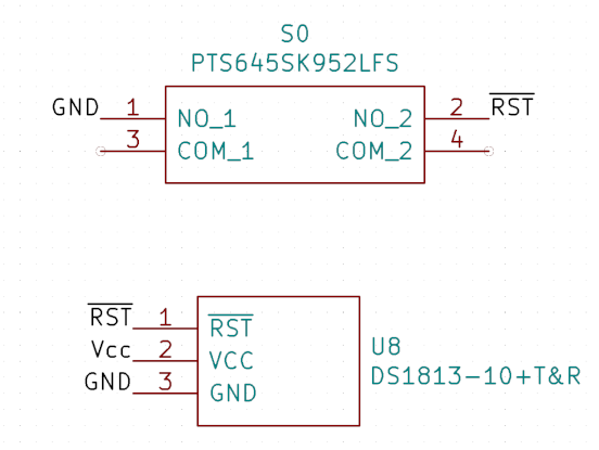
so what diode should i choose? i know there are different types and that they all have different values like breakdown voltage, voltage drop, etc. but i'm not sure if any of those are really important
Your 1N400x would not be good for digital signals, but I'm sure it's totally fine for the reset circuit.