
The cheap DIP sockets probably won't give you a reliable contact to the chip anymore after 10 plugging/unplugging cycles.
Precision DIP sockets are more robust and reliable, but they also cost more money.
Don't know an inexpensive source for precision DIP sockets in the UK (less expensive than Farnell and Mouser that is), you better ask somebody from the UK.
In Germany, I would order mpe GARRY sockets at Schukat,
but Schukat only sells to companies (not to private end users), and the prices at the Schukat homepage are without the VAT.
My6502 - A 74-Series 6502
-
GARTHWILSON

- Forum Moderator
- Posts: 8773
- Joined: 30 Aug 2002
- Location: Southern California
- Contact:
Re: My6502 - A 74-Series 6502
ttlworks wrote:
The cheap DIP sockets probably won't give you a reliable contact to the chip anymore after 10 plugging/unplugging cycles.
Precision DIP sockets are more robust and reliable, but they also cost more money.
Precision DIP sockets are more robust and reliable, but they also cost more money.
http://WilsonMinesCo.com/ lots of 6502 resources
The "second front page" is http://wilsonminesco.com/links.html .
What's an additional VIA among friends, anyhow?
The "second front page" is http://wilsonminesco.com/links.html .
What's an additional VIA among friends, anyhow?
Re: My6502 - A 74-Series 6502
ZIF (zero insertion force) sockets tend to be expensive, they tend to take a lot of space on the PCB,
but for EPROMs which are supposed to be plugged/unplugged quite often they are a good choice.
While looking around at mpe GARRY, I had stumbled over the 047 series of sockets.
They take less PCB space, and maybe they are less expensive... maybe not...
IIRC I have seen sockets like that in CNC controllers back in the 90s,
but don't ask me how/where to buy them.
Part numbers:
047-1-032-6-X0ZTX-ZT0 //Sn plated
047-1-032-6-X0ZFX-ZT0 //Au plated
;---
Fischer Elektronik also has nice sockets and connectors, but they won't be cheap.
but for EPROMs which are supposed to be plugged/unplugged quite often they are a good choice.
While looking around at mpe GARRY, I had stumbled over the 047 series of sockets.
They take less PCB space, and maybe they are less expensive... maybe not...
IIRC I have seen sockets like that in CNC controllers back in the 90s,
but don't ask me how/where to buy them.
047-1-032-6-X0ZTX-ZT0 //Sn plated
047-1-032-6-X0ZFX-ZT0 //Au plated
;---
Fischer Elektronik also has nice sockets and connectors, but they won't be cheap.
Re: My6502 - A 74-Series 6502
I'm curious about the 16-bit inc/dec circuit used in the C74.
One of the things I want to avoid is using multiple clocks to do a simple increment. In my current design, the self-counting registers make use of a binary counter chip like the 74HC161, which can act as both the register and the counter in one, so all I need do is assert count enable and on the clock rising edge the increment will happen. It also allows me to chain PCL and PCH so that PCH is incremented automatically when PCL rolls over, and I don't require a separate PCH_INC microcode instruction.
That said, the disadvantages are that I need a different circuit for these registers (or to design a more complex circuit that can mix and match chips), and that the up/down chips available to me, the '191 and '193 have completely incompatible (and frankly horrible) pinouts compared to the nice layout of the '161. Therefore the stack pointer would either need its own board design to use the '191 or a roll-my-own up/down counter using 2 '283 adders, or make use of the ALU to do its counting. This would take more cycles to achieve since it would require a register output, an ALU output and a register load.
The 16-bit inc/dec solution would mean that all my registers use the same circuit and chips, which is nice and elegant. But this circuit is essentially a mini AU (ALU minus the L!) so I'm wondering if it's possible to do the round trip in a single half cycle. Here's how I think it might work:
- Count Micro Instruction; Clock is LOW
- Register outputs to a special purpose 16-bit bus
Operand set in the inc/dec circuit ($01 or $FF)
Adders do their thing
- Inc/dec circuit latches the result
- inc/dec circuit outputs to the special bus
- Register latches its new value
- Register outputs to a special purpose 16-bit bus
Re: My6502 - A 74-Series 6502
Hmm... now you have opened a can of worms.
Depending on the speed of your CPU, and on the propagation delay of your ALU (and incrementer/decrementer etc.), there are different approaches to this.
C74 deliberately is aiming for speed. IIRC it has 2:1 multiplexers at the inputs of the registers PC, S, ADH\ADL,
so the registers individually could be either written from the ALU output or from the incrementer\decrementer (which is fed by the CPU internal address bus),
at the falling edge of PHI2.
;---
In theory, the idea to use a 16 Bit ALU able to run at twice the speed of the external CPU bus and to use it for incrementing/decrementing registers
during PHI2=low and to do data calculations during PHI2=high sounds nice, but the timing of the CPU external address bus has to be considered:
If the address changes too fast after the falling edge of PHI2, write cycles might be getting corrupted.
If the address changes too slow after the falling edge of PHI2, this gives the address decoding logic outside the CPU less time to do the job.
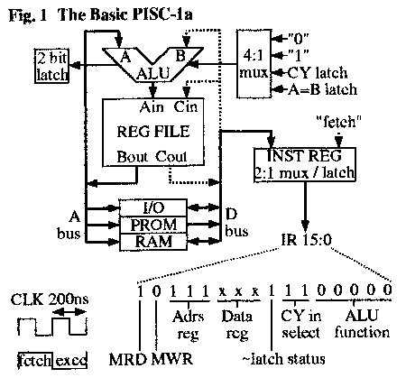
Back in 1994, Bradford J. Rodriguez introduced the PISC1:
One could replace the box labelled REG FILE with dual port RAM,
but the architecture would have to be modified a bit because for the 6502: data bus is 8 Bits and address bus is 16 Bits.
Unfortunately, the only manufacturer for that sort of dual port RAMs nowaday seems to be IDT, and it's hard to tell for how long these chips will stay in production.
;---
If your 8 Bit ALU would be really fast and your CPU external bus would be really slow, and you would be able to do 4 clock cycles inside the CPU for every bus cycle,
when pulling some tricks this would give a rather simple architecture like in my first TTL CPU (the mill would resemble something like a PIC16C54 microcontroller),
but back then I didn't know what I know now.
Also, for at least half of the time the ALU would be sitting idle, and the microcode would be getting somewhat bloated because the CPU core
has to run 4 times faster than the external bus (4 microcode cycles per 6502 machine cycle, that is).
;---
A different approach would be using 74ALS867\74ALS869 8 Bit synchronous up/down counters,
but they are very exotic, they are expensive, and it's hard to tell for how long these chips will stay in production.
Depending on the speed of your CPU, and on the propagation delay of your ALU (and incrementer/decrementer etc.), there are different approaches to this.
C74 deliberately is aiming for speed. IIRC it has 2:1 multiplexers at the inputs of the registers PC, S, ADH\ADL,
so the registers individually could be either written from the ALU output or from the incrementer\decrementer (which is fed by the CPU internal address bus),
at the falling edge of PHI2.
;---
In theory, the idea to use a 16 Bit ALU able to run at twice the speed of the external CPU bus and to use it for incrementing/decrementing registers
during PHI2=low and to do data calculations during PHI2=high sounds nice, but the timing of the CPU external address bus has to be considered:
If the address changes too fast after the falling edge of PHI2, write cycles might be getting corrupted.
If the address changes too slow after the falling edge of PHI2, this gives the address decoding logic outside the CPU less time to do the job.
Back in 1994, Bradford J. Rodriguez introduced the PISC1:
One could replace the box labelled REG FILE with dual port RAM,
but the architecture would have to be modified a bit because for the 6502: data bus is 8 Bits and address bus is 16 Bits.
Unfortunately, the only manufacturer for that sort of dual port RAMs nowaday seems to be IDT, and it's hard to tell for how long these chips will stay in production.
;---
If your 8 Bit ALU would be really fast and your CPU external bus would be really slow, and you would be able to do 4 clock cycles inside the CPU for every bus cycle,
when pulling some tricks this would give a rather simple architecture like in my first TTL CPU (the mill would resemble something like a PIC16C54 microcontroller),
but back then I didn't know what I know now.
Also, for at least half of the time the ALU would be sitting idle, and the microcode would be getting somewhat bloated because the CPU core
has to run 4 times faster than the external bus (4 microcode cycles per 6502 machine cycle, that is).
;---
A different approach would be using 74ALS867\74ALS869 8 Bit synchronous up/down counters,
but they are very exotic, they are expensive, and it's hard to tell for how long these chips will stay in production.
Last edited by ttlworks on Wed Dec 18, 2019 6:52 am, edited 1 time in total.

Re: My6502 - A 74-Series 6502
vfxsoup wrote:
so I'm wondering if it's possible to do the round trip in a single half cycle.
You can get away with using the ALU for SP, but PC really benefits from dedicated increment circuitry — either as a counter itself, or an external incrementer. This is because the 6502 overlaps the instruction fetch with ALU operations. The last cycle of ADC, for example, will store the result of the ALU, read the next opcode, and increment PC all at the same time.
On the other hand, if you are not concerned with cycle-accuracy, then by all means add extra cycles and use the main ALU to increment PC. You can even do it as two distinct 8-bit operations if necessary.
In the end, there are various design choices here depending on what you’re after.
C74-6502 Website: https://c74project.com

Re: My6502 - A 74-Series 6502
ttlworks wrote:
Back in 1994, Bradford J. Rodriguez introduced the PISC1:
The box labelled REG FILE is a set of eight, 8x2, 74172 multi-port register files, arrayed width-wise to accommodate 16-bit words. Eight words are stored, and, amazingly, it is a four-port device. By modern standards it is slow and power-hungry, but the 74172 can do two reads and two writes every cycle.
I bought a bunch of 74172's in the 1980's but my plans were a little too grand, and the project never got built. If anybody thinks they'd like to adopt some 172's to make a PISC -- or a 74-Series 6502 ! -- then drop me a PM and be prepared to convince me you're serious and they'd be going to a good home.
-- Jeff
In 1988 my 65C02 got six new registers and 44 new full-speed instructions!
https://laughtonelectronics.com/Arcana/ ... mmary.html
https://laughtonelectronics.com/Arcana/ ... mmary.html
Re: My6502 - A 74-Series 6502
Andrew Holme had used AM29705 16*4Bit dual port RAMs as REG FILE for building his Mark 2 FORTH Computer.
Bitsavers: AMD 2900 family, 1979, AM29705 datasheet is on PDF page 350 (2-342).
Ebay:
AM29705 $10, but no AM29334 (64*18Bit dual port RAM).
AM2903 $13, but no AM29203. //4 Bit bitslice
AM29C116 $20. //16Bit ALU plus registers.
No AM29332. //32Bit ALU
Oh... my... god: AM29325 $500, that's dirt cheap. But who would need a 32 Bit floating point ECL ALU (with TTL compatible pins) running at an 80ns machine cycle or such.
Sorry I got carried away, now back on topic:
74HCT670 is a 4*4Bit register file, separate read and write port. //74LS670 might be cheaper.
But again it's hard to tell for how long that chip will stay in production, and building a useful 16Bit register file might take a lot of chips.
Re: My6502 - A 74-Series 6502
Thanks for the replies and explanations all. Very interesting, and a lot to digest.
I'm thinking that this will take my design in a different direction to how I'd planned so I think I'll design a hybrid static/inc-only register card that will house two registers per card (A+T, X+Y, PCL+PCH, ADL+ADH), and a separate card that will house the stack (based around the '191) and status registers. it's a shame that there aren't any HC 8-bit counters like the one you linked to Dieter - such a chip would be perfect for all the counter registers.
I'm thinking that this will take my design in a different direction to how I'd planned so I think I'll design a hybrid static/inc-only register card that will house two registers per card (A+T, X+Y, PCL+PCH, ADL+ADH), and a separate card that will house the stack (based around the '191) and status registers. it's a shame that there aren't any HC 8-bit counters like the one you linked to Dieter - such a chip would be perfect for all the counter registers.
Re: My6502 - A 74-Series 6502
74ALS569 is a 4 Bit up/down counter with output enable, but again:
It's pretty exotic, it isn't available as HCT, and it's hard to tell for how long that chip will stay in production.
No other 8 Bit up/down counters so far which have 8 inputs and 8 outputs, and using GAL22V10 as a counter would be cheating.
Ordering a lot of identical PCBs would lower the price per PCB, but the 74244 pinout isn't ideal for 4 Bit bitslice.
BTW: Counters also could be used as registers only (and not just for counting).
Re: My6502 - A 74-Series 6502
ttlworks wrote:
Ordering a lot of identical PCBs would lower the price per PCB, but the 74244 pinout isn't ideal for 4 Bit bitslice.
Quote:
BTW: Counters also could be used as registers only (and not just for counting).
Re: My6502 - A 74-Series 6502
8 Bit 74377 latch has load with synchronous enable, but no clear.
4 Bit 74161\74163 counter has load with synchronous enable, and a clear input.
So if one needs an 8 Bit latch with 'load with synchronous enable' and 'clear',
but there is no 8 Bit latch chip which features both,
one could use two 74161\74163 4 Bit counters instead.
There are two approaches:
Either building a set of register cards which feature two 16 Bit registers per card (what you had suggested),
or building a set of four bitslice cards which feature 4 Bits for all of the registers (since you would be using quite a few 4 Bit counters anyway).
4 Bit 74161\74163 counter has load with synchronous enable, and a clear input.
So if one needs an 8 Bit latch with 'load with synchronous enable' and 'clear',
but there is no 8 Bit latch chip which features both,
one could use two 74161\74163 4 Bit counters instead.
vfxsoup wrote:
Any reason why you're mentioning the '244?
Either building a set of register cards which feature two 16 Bit registers per card (what you had suggested),
or building a set of four bitslice cards which feature 4 Bits for all of the registers (since you would be using quite a few 4 Bit counters anyway).
Re: My6502 - A 74-Series 6502
ttlworks wrote:
So if one needs an 8 Bit latch with 'load with synchronous enable' and 'clear'
Re: My6502 - A 74-Series 6502
Nah, that's just an example of "how to keep going with the chips that are available".
I think you won't need clearing a register to zero for building a 6502, but we might be getting there again when generating a video signal...
...or when building peripherals for the CPU.
BTW: before trying to make PCB layouts, it's usual to spend some days with paper and pencil to get a better clue about how/where/why to place the chips.
IMHO it probably would make sense to consider both approaches (16 Bit cards versys bitslice cards), just to see which approach gives more simple PCB layouts.
Anyhow, for better signal integrity the bus interface would be 8 Bit / 16 Bit and located on the motherboard or such.
Hmm... I better should warn you from the start that routing a PCB layout isn't a "one way street",
sometimes the schematics have to be changed to give simpler PCB layouts.
Like swapping two inputs of a logic gate, or swapping two identical logic gates within a chip, or swapping two identical logic gates between two chips,
or swapping the Bit order of buffers and latches...
In "case of emergency" one also could swap the Bit order of the address lines or of the data lines of a RAM.
It works less good for ROMs, because then one would need to write a little bit of C code that modifies the binary to be burned into the ROM accordingly
(sort of a weak "copyright protection").
-
GARTHWILSON
- Forum Moderator
- Posts: 8773
- Joined: 30 Aug 2002
- Location: Southern California
- Contact:
Re: My6502 - A 74-Series 6502
vfxsoup wrote:
So here's a potentially silly question but does a 6502 clear all its registers to zero on reset? Does it matter? Just wondering since you'd explicitly set a register to the value you want during a program, or would you assume, for example, that X or Y are automatically zero (that seems dangerous to me)?
http://WilsonMinesCo.com/ lots of 6502 resources
The "second front page" is http://wilsonminesco.com/links.html .
What's an additional VIA among friends, anyhow?
The "second front page" is http://wilsonminesco.com/links.html .
What's an additional VIA among friends, anyhow?