I wanted to introduce my 6502 project, which I'm going to start building in hardware in the new year.
I'm a Visual Effects Supervisor for films and TV, previously a programmer and dev-manager. I have no training in electronics whatsoever outside of what we covered in school, and that's going back 28 years. Like many people I was hooked by Ben Eater's series on YouTube; One day I absentmindedly wondered about how you'd go about adding two numbers together using simple logic, and that led me to Ben's videos. Considering I'd been using computers all my life (VIC20, C64, Amiga for anyone interested) I was quite ignorant of how MPUs actually worked, so needless to say it was a real mind-blow moment when his SAP1 computer started doing stuff, and my reaction was "I've got to build me one of those!" I'd planned to build the same SAP1 computer in the same way (breadboards) but somehow the idea of a 16-byte computer with a seven-segment display output didn't stretch me enough (and I quickly got bored bending wires). So I thought I'll have 32kb RAM and I'll use one of those multi-line LCD displays, and make a PCB like the Gigatron. Oh, and I'll make the instruction set based on that of the 6502, but just a small subset - none of the weird addressing modes, or interrupts, or anything complicated like that...
And then I discovered the C74 thread here at 6502.org.
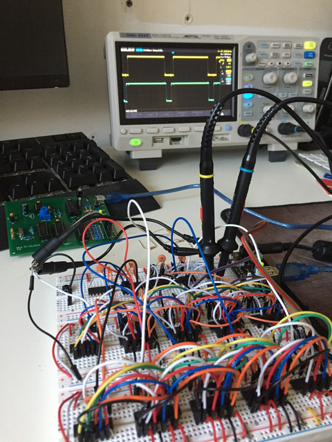
Up to this point I'd been struggling to get some of the instructions to fit within 8-steps, as I was still basing the design around the single bus of the SAP1, but Drass's dual R/W bus architecture freed up this constraint, and so I decided to base my project on that. However I didn't want to just copy it outright, as this was, is and always will be a learning exercise for me, so I've been on quite a journey learning how to construct the instructions and shape the architecture accordingly.
Some months ago, a YouTuber David Barr, aka OneLoneCoder or javidx9 (check out his channel - he's brilliant) started a NES emulator project. Of course this is 6502-based and it gave me the idea to plan my project out using an emulation of my own. While his is very high-level, mine had to be at the control wire level since it would directly influence the design of the microcode and its storage strategy. I decided to use Processing (processing.org), which is a Java-based framework for building graphical applications. I'm pretty good with C++ but Processing provides the graphical functions out of the box, making it easy to experiment.
Here's the latest version ready to run that right-of-passage program that all homebrew TTL computers seem to do - the Fibonacci Sequence.
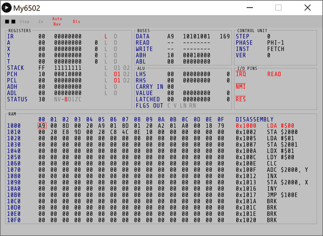
There's quite a lot of information packed into that small window! The two squares at the top left represent the two clock phases; the most recent addition was the disassembler next to the memory display. I have successfully implemented about 50% of all MOS 6502 opcodes. There's something for each instruction, and all addressing modes are present. So far it's also cycle accurate, in that if an instruction is meant to take 5 cycles, it takes 5 cycles. Although I have BRK working, the hardware interrupts aren't yet wired up so hitting I or N won't do anything other than toggle the state of the "pins". It's extremely slow (about 5Hz!) but it's written to help me design the hardware rather than for raw power! I'm pretty pleased with it, and will share the code on GitHub when I'm happy that it's shareable (bit of a mess at the moment).
It's been a heck of a learning curve! It seems like the microcode ROM layout has had to be tweaked with almost every new addressing mode or instruction, and this in turn has affected the overall design. But at long last (and thanks to Dieter for his weekly prods!) I think I have a design that will translate into a hardware build.
This is the overview:
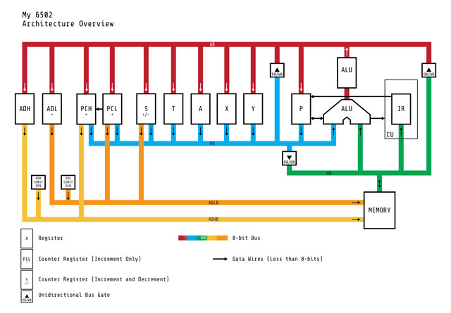
So as I said it's based on Drass's design (thank you Drass), but with some notable differences:
- The ALU takes its inputs directly from the RB and DB, and doesn't have a B-input Register. It has an output register that latches every half cycle with whatever's in the ALU result
- The S, PC and ADL are all "self-counting" registers, that will be based on 74HC191 (Stack) and 74HC161 (Others) chips
- There's a "gate" that links the RB to the WB, allowing for example the Accumulator to output and the X-reg to load in the same half-cycle without using the ALU
- The Address Buses are output directly from the PC, AD and S registers
- The ADL constant generator can output $FA, $FB, $FC, $FD, $FE and $FF rather than just the even values (this was a recent change after I realised that I had no efficient way of adding one to the even values!)
- There's no support for Decimal mode. It's just one control line too many for me to fit it into my ROMs at the moment!
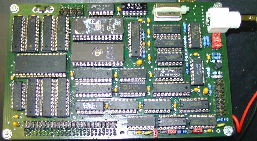
At the moment I have no intention of ever connecting this to a VIC20 or C64, in fact it will be part of a unique computer all of its own, which will include a VGA output. I'm hoping it will run at about 1.56MHz (divided from the 12.5MHz pixel clock of the monitor output), or 3.125MHz internally (when clock is split into its two phases). I've managed to squeeze a 65-bit control word into two 16-bit ROMs (or Flash memory as it will be initially), and the whole thing, except for the Flash memory chips will be through-hole for that extra retro feel. Each component will have its own card, complete with LEDs for a cool light show, and for debugging in single-step mode of course. I'm hoping that by the time it's all built that my children (currently 3 years and 8 months) will marvel at this beast and be able to learn about how computers work.
So that's my project - I think this post is long enough for now. Please stay tuned for updates (but please also be patient - I have limited time at the moment to spend on it), and feel free to ask any questions/make any suggestions/scoff at my bizarre choices. This is an amazing resource for retro computing enthusiasts, and it's been invaluable to me over the past months while I've been figuring this all out.
Christian