6502.org Forum  Projects  Code  Documents  Tools  Forum
It is currently Fri Nov 22, 2024 3:56 pm

All times are UTC


Post new topic Reply to topic  [ 67 posts ]  Go to page 1, 2, 3, 4, 5  Next
Author Message
PostPosted: Wed Dec 11, 2019 3:27 pm 
Offline

Joined: Mon Sep 30, 2019 1:33 pm
Posts: 34
Hi all,

I wanted to introduce my 6502 project, which I'm going to start building in hardware in the new year.

I'm a Visual Effects Supervisor for films and TV, previously a programmer and dev-manager. I have no training in electronics whatsoever outside of what we covered in school, and that's going back 28 years. Like many people I was hooked by Ben Eater's series on YouTube; One day I absentmindedly wondered about how you'd go about adding two numbers together using simple logic, and that led me to Ben's videos. Considering I'd been using computers all my life (VIC20, C64, Amiga for anyone interested) I was quite ignorant of how MPUs actually worked, so needless to say it was a real mind-blow moment when his SAP1 computer started doing stuff, and my reaction was "I've got to build me one of those!" I'd planned to build the same SAP1 computer in the same way (breadboards) but somehow the idea of a 16-byte computer with a seven-segment display output didn't stretch me enough (and I quickly got bored bending wires). So I thought I'll have 32kb RAM and I'll use one of those multi-line LCD displays, and make a PCB like the Gigatron. Oh, and I'll make the instruction set based on that of the 6502, but just a small subset - none of the weird addressing modes, or interrupts, or anything complicated like that...

And then I discovered the C74 thread here at 6502.org.

Up to this point I'd been struggling to get some of the instructions to fit within 8-steps, as I was still basing the design around the single bus of the SAP1, but Drass's dual R/W bus architecture freed up this constraint, and so I decided to base my project on that. However I didn't want to just copy it outright, as this was, is and always will be a learning exercise for me, so I've been on quite a journey learning how to construct the instructions and shape the architecture accordingly.

Some months ago, a YouTuber David Barr, aka OneLoneCoder or javidx9 (check out his channel - he's brilliant) started a NES emulator project. Of course this is 6502-based and it gave me the idea to plan my project out using an emulation of my own. While his is very high-level, mine had to be at the control wire level since it would directly influence the design of the microcode and its storage strategy. I decided to use Processing (processing.org), which is a Java-based framework for building graphical applications. I'm pretty good with C++ but Processing provides the graphical functions out of the box, making it easy to experiment.

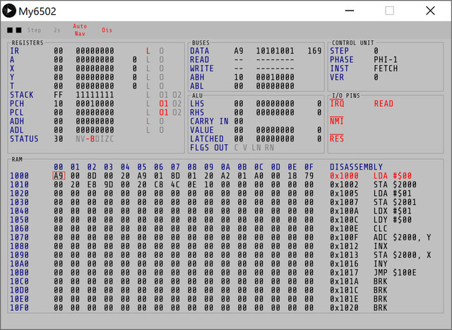
Here's the latest version ready to run that right-of-passage program that all homebrew TTL computers seem to do - the Fibonacci Sequence.
Image

There's quite a lot of information packed into that small window! The two squares at the top left represent the two clock phases; the most recent addition was the disassembler next to the memory display. I have successfully implemented about 50% of all MOS 6502 opcodes. There's something for each instruction, and all addressing modes are present. So far it's also cycle accurate, in that if an instruction is meant to take 5 cycles, it takes 5 cycles. Although I have BRK working, the hardware interrupts aren't yet wired up so hitting I or N won't do anything other than toggle the state of the "pins". It's extremely slow (about 5Hz!) but it's written to help me design the hardware rather than for raw power! I'm pretty pleased with it, and will share the code on GitHub when I'm happy that it's shareable (bit of a mess at the moment).

It's been a heck of a learning curve! It seems like the microcode ROM layout has had to be tweaked with almost every new addressing mode or instruction, and this in turn has affected the overall design. But at long last (and thanks to Dieter for his weekly prods!) I think I have a design that will translate into a hardware build.

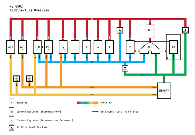
This is the overview:
Image

So as I said it's based on Drass's design (thank you Drass), but with some notable differences:
- The ALU takes its inputs directly from the RB and DB, and doesn't have a B-input Register. It has an output register that latches every half cycle with whatever's in the ALU result
- The S, PC and ADL are all "self-counting" registers, that will be based on 74HC191 (Stack) and 74HC161 (Others) chips
- There's a "gate" that links the RB to the WB, allowing for example the Accumulator to output and the X-reg to load in the same half-cycle without using the ALU
- The Address Buses are output directly from the PC, AD and S registers
- The ADL constant generator can output $FA, $FB, $FC, $FD, $FE and $FF rather than just the even values (this was a recent change after I realised that I had no efficient way of adding one to the even values!)
- There's no support for Decimal mode. It's just one control line too many for me to fit it into my ROMs at the moment!

At the moment I have no intention of ever connecting this to a VIC20 or C64, in fact it will be part of a unique computer all of its own, which will include a VGA output. I'm hoping it will run at about 1.56MHz (divided from the 12.5MHz pixel clock of the monitor output), or 3.125MHz internally (when clock is split into its two phases). I've managed to squeeze a 65-bit control word into two 16-bit ROMs (or Flash memory as it will be initially), and the whole thing, except for the Flash memory chips will be through-hole for that extra retro feel. Each component will have its own card, complete with LEDs for a cool light show, and for debugging in single-step mode of course. I'm hoping that by the time it's all built that my children (currently 3 years and 8 months) will marvel at this beast and be able to learn about how computers work.

So that's my project - I think this post is long enough for now. Please stay tuned for updates (but please also be patient - I have limited time at the moment to spend on it), and feel free to ask any questions/make any suggestions/scoff at my bizarre choices. This is an amazing resource for retro computing enthusiasts, and it's been invaluable to me over the past months while I've been figuring this all out.

Christian

Last edited by vfxsoup on Thu Dec 12, 2019 12:47 pm, edited 1 time in total.

Top
 Profile  
Reply with quote  
PostPosted: Wed Dec 11, 2019 4:20 pm 
Offline
User avatar

Joined: Fri Nov 09, 2012 5:54 pm
Posts: 1431
Looks nice for a start.

The disadvantage of not having a B register is,
that the propagation delays of memory plus ALU will add up,
and this will put a limit to the speed of your CPU.

Your block diagram somehow reminds me a bit to the 65CE02.

Image


Top
 Profile  
Reply with quote  
PostPosted: Thu Dec 12, 2019 12:26 am 
Offline
User avatar

Joined: Sat Dec 01, 2018 1:53 pm
Posts: 730
Location: Tokyo, Japan
vfxsoup wrote:
...and will share the code on GitHub when I'm happy that it's shareable (bit of a mess at the moment).
From what I've seen, the vast majority of code that starts out this way is never shared. I would strongly encourage you to just get your git repo up there now (if you have no repo, immediately `make clean` and run `git init && git add . && git commit -m 'Initial commit'`) and worry about cleaning it up later.

I'm still pretty disappointed that we lost all the code for a pretty neat Python 6502 emulating disassembler that the Robotron disassembly guy was doing because the project eventually faded away before he made any of the code available.

_________________
Curt J. Sampson - github.com/0cjs


Top
 Profile  
Reply with quote  
PostPosted: Thu Dec 12, 2019 6:58 am 
Offline
User avatar

Joined: Fri Nov 09, 2012 5:54 pm
Posts: 1431
Christian, now to go through your block diagram from left to right:

ADL is implemented with 74161 counters, ADH is not. //Obviously you are going to need this for addressing modes like (IND),Y \ (IND,X) and JMP (ABS).
NMOS 6502 does not increment ADH for JMP ($00FF), 65C02 does, so to me it looks like you are aiming for the NMOS 6502 instruction set.

That arrow from PCL to PCH is a thing I haven't seen yet, I'm interested to see some microcode related to this.

About S: the 74191 up\down counter is less good than the 74LS169 (which would better fit to the 74161),
but 74169 is only available as LS from TI, and it's hard to tell for how long the 74169 will stay in production.
It's an interesting question, if JSR and BRK still would fit into 8 machine cycles when implementing S with 74161 up counters and decrementing S by the ALU.
BTW: when it comes to push/pull, 6502 does pre_increment and post_decrement (like 6800), not pre_decrement and post_increment (like 6809 and 68k).
Means that S will always point to an empty location on the stack.
I wasn't aware about this from the start when building my first TTL CPU.

In our 20MHz TTL CPU, we had to bypass the ALU with a buffer for getting cycle\timing compatible to the NMOS 6502.
Whether you are going to need that ALU bypass or not depends on your intentions and on your ALU design.

Speaking of it, I'm interested to hear how you are going to implement the ALU,
especially the "shift right" operation at the ALU output.

In the status register, B isn't really a flag, it's a status Bit from the instruction decoder\sequencer to be pushed on the stack during a BRK instruction or an interrupt sequence.
I wasn't aware about that when building my first TTL CPU, too.

Would be better to have some reserved/unused Bits in the outputs of the microcode ROMs,
during the building process of Drass's CPU we always seemed to had a few Bits too few there.

It might be more economical to do an instruction fetch at the end of a microcode sequence,
also it's better (more safe) if the CPU hardware defaults to fetching the next instruction for empty locations ($FF) in the microcode ROM.

If there are bugs in the CPU after building the hardware, they mostly seem to be related to the microcode (but the simulation would catch them),
or to clock generation and timing (so we better take a closer look at these details in your design later).

Hmm... to me, it looks now like the VGA display generator isn't a part of the CPU core.
Would be nice if you could tell us how you would like to build that part of your computer.

Cheers,
Dieter.


Top
 Profile  
Reply with quote  
PostPosted: Thu Dec 12, 2019 12:10 pm 
Offline

Joined: Mon Sep 30, 2019 1:33 pm
Posts: 34
cjs wrote:
vfxsoup wrote:
...and will share the code on GitHub when I'm happy that it's shareable (bit of a mess at the moment).
From what I've seen, the vast majority of code that starts out this way is never shared. I would strongly encourage you to just get your git repo up there now (if you have no repo, immediately `make clean` and run `git init && git add . && git commit -m 'Initial commit'`) and worry about cleaning it up later.

I'm still pretty disappointed that we lost all the code for a pretty neat Python 6502 emulating disassembler that the Robotron disassembly guy was doing because the project eventually faded away before he made any of the code available.


Consider it done!

https://github.com/christianlett/proces ... ter/My6502

As I said it's a bit of a mess, and still very much under development so please don't judge too harshly :D

You'll need to download the latest build of Processing from [url]processing.org/download[/url]

Download all the files from the repo, including the "data" directory, and open the My6502.pde file.


Top
 Profile  
Reply with quote  
PostPosted: Thu Dec 12, 2019 12:47 pm 
Offline

Joined: Mon Sep 30, 2019 1:33 pm
Posts: 34
ttlworks wrote:
Christian, now to go through your block diagram from left to right:
ADL is implemented with 74161 counters, ADH is not. //Obviously you are going to need this for addressing modes like (IND),Y \ (IND,X) and JMP (ABS).
NMOS 6502 does not increment ADH for JMP ($00FF), 65C02 does, so to me it looks like you are aiming for the NMOS 6502 instruction set.

Correct - I'm implementing only the NMOS 6502 instructions.
ADH is not a Counter Register at the moment. For the (ind, X) and (ind), Y instructions I've written so far the high address goes through the ALU.

Quote:
That arrow from PCL to PCH is a thing I haven't seen yet, I'm interested to see some microcode related to this.

That is simply the carry out from the PCL counter to the PCH counter that increments when PCL goes above 255.

Quote:
About S: the 74191 up\down counter is less good than the 74LS169 (which would better fit to the 74161),
but 74169 is only available as LS from TI, and it's hard to tell for how long the 74169 will stay in production.

The 191 has a horrible pinout, but that aside it could be the chip to use for all the counter registers, since it can be set to count up permanently. I have lots of 161s but they'll be put to good use in the video adapter (more on that later). I'd not even seen the 169, since I've only been looking at the HC and AC flavour chips. Still, might be worth getting hold of a couple of 169s and doing some experiments to see how they might interface with the non-TTL chips.

Quote:
It's an interesting question, if JSR and BRK still would fit into 8 machine cycles when implementing S with 74161 up counters and decrementing S by the ALU.

Definitely worth a look.

Quote:
BTW: when it comes to push/pull, 6502 does pre_increment and post_decrement (like 6800), not pre_decrement and post_increment (like 6809 and 68k).
Means that S will always point to an empty location on the stack.
I wasn't aware about this from the start when building my first TTL CPU.

Checks code... Yes that's what I'm doing. The SP is initialised to $FF and on a push I write to that location then decrement. Therefore to pull I need to increment first before reading from the stack memory.

Quote:
In our 20MHz TTL CPU, we had to bypass the ALU with a buffer for getting cycle\timing compatible to the NMOS 6502.
Whether you are going to need that ALU bypass or not depends on your intentions and on your ALU design.
Speaking of it, I'm interested to hear how you are going to implement the ALU, especially the "shift right" operation at the ALU output.

The bypass buffer is just a convenient way of getting data from the DB to the WB in the same cycle, and seemed like a common sense thing to have. The ALU will be based on your multiplexer design. I've not yet laid out the shifter logic, but I believe it will use an 8-bit buffer (like the 74HC541) with its outputs offset by one bit, and the MSB will either be connected to the carry in, or to ground depending on the instruction. Of course I also need to consider what happens when NOT making use of a shift right operation.

Quote:
In the status register, B isn't really a flag, it's a status Bit from the instruction decoder\sequencer to be pushed on the stack during a BRK instruction or an interrupt sequence.
I wasn't aware about that when building my first TTL CPU, too.

This is something I still need to figure out.

Quote:
Would be better to have some reserved/unused Bits in the outputs of the microcode ROMs, during the building process of Drass's CPU we always seemed to had a few Bits too few there.

Yes, I'm currently considering adding a third ROM to add another 8, or 16 bits of breathing room. Currently for example the shift-right control bit is hacked from the ALU's input bit pattern. As you'll know very well the combination of 4 bits gives various input combinations. I'm not using 0001 so intercept that to set the shift-right bit and then reset the input to 0000. It's a clever hack, but a hack nonetheless, and I'd much rather have a microcode instruction to set this properly.

Quote:
It might be more economical to do an instruction fetch at the end of a microcode sequence,
also it's better (more safe) if the CPU hardware defaults to fetching the next instruction for empty locations ($FF) in the microcode ROM.

At the moment the fetch is done at the start of the sequence. I'll need to get my head around how this would work doing it at the end because how does it fetch the first instruction?

Quote:
If there are bugs in the CPU after building the hardware, they mostly seem to be related to the microcode (but the simulation would catch them),
or to clock generation and timing (so we better take a closer look at these details in your design later).

Because this is a standalone computer I'm thinking about just generating a clock and call every other pulse PHI1 and the other PHI2. I admit that this is a rather naive way of doing it so I'll be interested in investigating this further.

Quote:
Hmm... to me, it looks now like the VGA display generator isn't a part of the CPU core.
Would be nice if you could tell us how you would like to build that part of your computer.

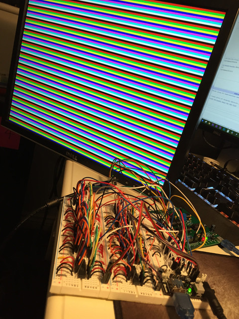
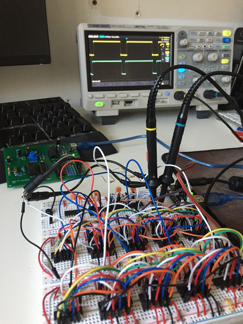
It's been a while since I looked at the video generator, but I do have a working breadboard circuit generating the correct timing for a 320x200 pixel output. Because the MPU clock speed is divided from the pixel clock I think I can read from memory at times when I know the MPU isn't reading or writing. I'll also be overlaying ROM for character/colour generation that only the video generator can read from. It's actually quite simple to do when you've got your head round the front and back porches, etc. :)

Image
Image

Thanks for the comments. Christian


Top
 Profile  
Reply with quote  
PostPosted: Thu Dec 12, 2019 1:28 pm 
Offline
User avatar

Joined: Fri Nov 09, 2012 5:54 pm
Posts: 1431
ttlworks wrote:
That arrow from PCL to PCH is a thing I haven't seen yet, I'm interested to see some microcode related to this.
vfxsoup wrote:
That is simply the carry out from the PCL counter to the PCH counter that increments when PCL goes above 255.

Ah, then I had misinterpreted this: to me, it somehow looked like data instead of a simple carry signal.

vfxsoup wrote:
doing some experiments to see how they might interface with the non-TTL chips.

74LS, 74HCT and 74ACT are supposed to have a logic level threshold of ca. 1.3V.
74HC and 74AC have a logic level threshold of half the supply voltage (2.5V at VCC=5V).

A 74LS output with some load to GND sometimes can't give out more than 2.5V,
so 74LS outputs driving 74HC\74AC inputs is a thing that should be avoided if possible.
//Adding pullup resistors to 74LS outputs to compensate for this sometimes isn't a "clean" solution.

vfxsoup wrote:
At the moment the fetch is done at the start of the sequence. I'll need to get my head around how this would work doing it at the end because how does it fetch the first instruction?

It might fetch the first instruction "at random" before going into the RESET sequence, but I think this isn't much of a problem.
Putting the instruction fetch at the end of the microcode sequence just simplifies the hardware a bit.
Would be interesting to try which of the two approaches for instruction fetching would be better for conditional branches in your design.

vfxsoup wrote:
It's been a while since I looked at the video generator, but I do have a working breadboard circuit generating the correct timing for a 320x200 pixel output.

I had cheated by using a lookup table in a ROM for generating display address and synch signals.
The address lines of the ROM were fed by a 74393 based counter running at 1MHz.

vfxsoup wrote:
Because the MPU clock speed is divided from the pixel clock I think I can read from memory at times when I know the MPU isn't reading or writing.

RAM used by the CPU during PHI2=HIGH and by a video chip or such during PHI2=LOW is quite common for 6502 computers.

Nice picture on the screen, somehow I never had made it to build a colour video generator.
On the bright side, my monochrome video generators were able to display text and graphics at the same time.

Attachment:
d04_blockdiagram.png
d04_blockdiagram.png [ 46.49 KiB | Viewed 3061 times ]


Image

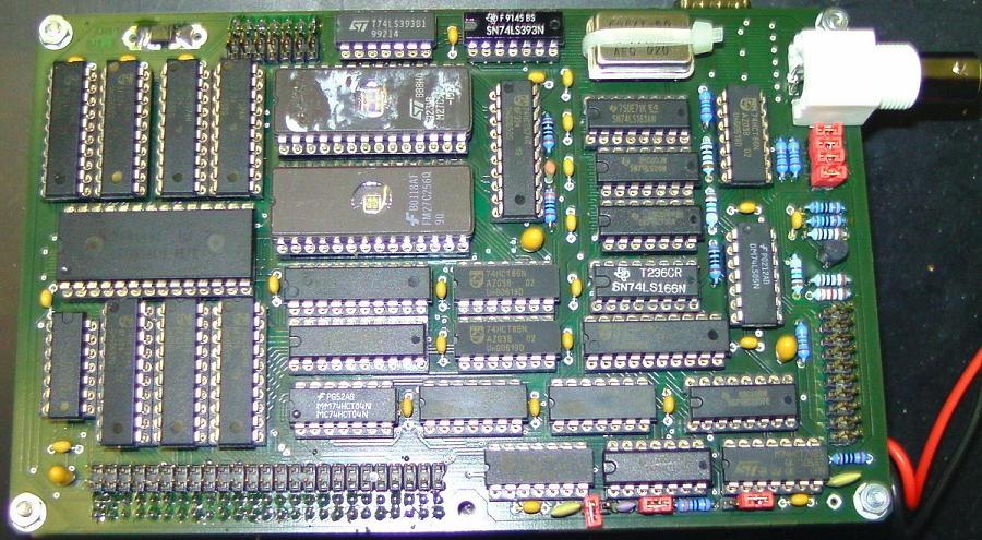
D04 was able to generate an analog video signal while driving a LCD, text and graphics were mixed together with XOR gates.
What had bloated the design a bit was passively snooping the 6502 bus for write cycles for mirroring them into the display RAM...
Screen resolution was monochrome 320*200.


Top
 Profile  
Reply with quote  
PostPosted: Thu Dec 12, 2019 1:51 pm 
Offline
User avatar

Joined: Sat Dec 01, 2018 1:53 pm
Posts: 730
Location: Tokyo, Japan
vfxsoup wrote:
Consider it done!
https://github.com/christianlett/proces ... ter/My6502
As I said it's a bit of a mess, and still very much under development so please don't judge too harshly :D
I'm judging you very highly for getting the code out there. Though I had a quick look at it and actually the code doesn't look at all messy to me.

And you might just drop these two lines into a README file in the repo:
Quote:
You'll need to download the latest build of Processing from [url]processing.org/download[/url]
Download all the files from the repo, including the "data" directory, and open the My6502.pde file.
(Don't worry about putting anything else in the README at the moment unless you have a strong urge; I just mention the above since you already wrote this documentation anyway.)

_________________
Curt J. Sampson - github.com/0cjs


Last edited by cjs on Thu Dec 12, 2019 2:06 pm, edited 1 time in total.

Top
 Profile  
Reply with quote  
PostPosted: Thu Dec 12, 2019 1:58 pm 
Offline
User avatar

Joined: Thu Dec 11, 2008 1:28 pm
Posts: 10985
Location: England
vfxsoup wrote:
cjs wrote:
... I would strongly encourage you to just get your git repo up there now

Consider it done!

Thanks for doing that - always good to see code shared, and indeed it's best not to wait until it's polished or final.


Top
 Profile  
Reply with quote  
PostPosted: Thu Dec 12, 2019 4:07 pm 
Offline

Joined: Mon Sep 30, 2019 1:33 pm
Posts: 34
I should probably mention that if you do download and run the emulation, you'll might find the following keyboard shortcuts useful:
- c or C runs and stops the clock
- SPACE single steps (half cycle)
- R resets
- 2 switches between 0-255 and -128-127 in some of the registers' decimal displays
- a or A toggles auto memory navigate (memory shows wherever the address buses point to)
- If auto memory navigate is turned off you can use the cursor keys to navigate the memory display (left/right go to the start and end, up/down to move between pages)
- d or D toggles between disassembly and the character view of the memory
- i or I toggles the IRQ line (doesn't do anything yet)
- n or N toggles the NMI line (ditto)


Top
 Profile  
Reply with quote  
PostPosted: Thu Dec 12, 2019 11:28 pm 
Offline
User avatar

Joined: Sun Oct 18, 2015 11:02 pm
Posts: 428
Location: Toronto, ON
vfxsoup wrote:
it's based on Drass's design (thank you Drass)
Thank you for the kind mention, and I’m so glad you found this helpful. (I hasten to add that this was a team effort, with ttlworks and Dr Jefyll).

Quote:
At the moment the fetch is done at the start of the sequence. I'll need to get my head around how this would work doing it at the end because how does it fetch the first instruction?
The fetch of the first opcode technically occurs at the end of the RESET sequence, and then again at the end of every instruction thereafter. (You can safely ignore what happens prior to /RES going high to trigger the RESET sequence). It's handy to implement it this way so the new opcode is clocked into the IR in time to index the microcode ROMs directly. The IR will then quite naturally point to the microcode sequence for the next opcode.

Note also that all (documented) 6502 instructions execute a FetchOperand micro-instruction in the cycle following FetchOpcode. (This is done even for single-byte instructions, and is why even a NOP takes two cycles, for example). As ttlworks points out, FetchOperand can simply load an ALU input register. This avoids having to complete a memory read *and* and an ALU operation in one cycle. It also makes things nice and regular for the first couple of steps of every instruction. (The C74-6502 exploits this regularity to implement the microcode pipeline).

Best of luck on your project!

_________________
C74-6502 Website: https://c74project.com


Top
 Profile  
Reply with quote  
PostPosted: Fri Dec 13, 2019 8:09 am 
Offline
User avatar

Joined: Fri Nov 09, 2012 5:54 pm
Posts: 1431
I'm not sure about the availability of the 74283 adder in the future.
Actually we have two ALU designs "on stock":
An ALU where multiplexers are built around 74283 adders, and a different ALU entirely built from multiplexers (plus a few XOR gates maybe).

Christian, if you want to do graphics on your computer, just a monochrome 320*200 picture takes 8000 Bytes in total.
With 32kB RAM, displaying only one 160*200 picture in color (two Bits per pixel) nearly eats up a quarter of the RAM.
Would suggest to take a look at the K24 concept.
It adds some registers for getting a 24 Bit address bus plus some 65816 addressing modes and instructions for making use of the 24 Bits.
Means, that software for K24 can be done with any 65816 assembler.
Downside is, that some of the instructions probably would take more than 8 microcode steps with your architecture.
Also, for K24 a RTI pops three address Bytes from stack, this causes a little incompatibility (monitor programs tend to use RTI for starting user code).
Switching between two sets of microcode can fix this, but this adds a bit to the complexity of the design.


Are you going to use SMD chips, or through hole parts ? //There are pros and cons for both.

;---

Another interesting question is, what software you are going to use for drawing the schematics and routing the PCB layouts.

I had started with Eagle back in 1998 or so, I always had liked it, and I always had advocated it. We have used it for the C74project.
But all this was before AutoDesk had acquired Eagle and switched it to the "subscription model" licensing scheme.
We have a problem with that, because you wouldn't rent a mission critical part of your infrastructure on a monthly basis.
So I had stopped with advocating Eagle.

I recently tried KiCad (free software), and I have to say that it had improved a lot over the past few years, it's certainly possible to work with it.
Some of the PCB manufacturers accept KiCad files, so there is a chance of getting around that Gerber conversion.
Looks like KiCad was used for designing the Gigatron.


Top
 Profile  
Reply with quote  
PostPosted: Sat Dec 14, 2019 11:26 am 
Offline

Joined: Mon Sep 30, 2019 1:33 pm
Posts: 34
ttlworks wrote:
I'm not sure about the availability of the 74283 adder in the future.

I have four 74HC283 ICs in my collection, so the ALU will be based around your multiplexer + adders design. I wonder if the stack pointer could be designed around two of these instead of the '191?

Quote:
Christian, if you want to do graphics on your computer, just a monochrome 320*200 picture takes 8000 Bytes in total.

The display will work similarly to the VIC-II so will be primarily character based (1000 bytes, with the character bitmaps in ROM). I was working on allowing each character to have its own background colour as well as a unique foreground colour. If I only have 16 colours then I can achieve this in the 1000 byte colour RAM, but it's still under consideration. I'm not fully sure about bitmap modes yet, but if I do it will probably ape the VIC-II so that colour mode down-res's to 160x200.

Quote:
Are you going to use SMD chips, or through hole parts ? //There are pros and cons for both.

I have about 200 DIP through hole chips. I like the aesthetic!

Quote:
Another interesting question is, what software you are going to use for drawing the schematics and routing the PCB layouts.

At the moment I'm using EasyEDA but it has obvious limitations as it's web-based. I have played with KiCad, so will ultimately move over to using that I think.


Top
 Profile  
Reply with quote  
PostPosted: Mon Dec 16, 2019 8:59 am 
Offline
User avatar

Joined: Fri Nov 09, 2012 5:54 pm
Posts: 1431
Quote:
I have four 74HC283 ICs in my collection, so the ALU will be based around your multiplexer + adders design. I wonder if the stack pointer could be designed around two of these instead of the '191?

Certainly yes, one could implement the stack pointer by resorting to two 74283 adders and a register.
One also could attach four 74283 adders to the CPU internal 16 Bit address bus to work as a 16 Bit incrementer/decrementer and go without the 74161\74191 counters. ;)

Quote:
I have about 200 DIP through hole chips. I like the aesthetic!

DIP simplifies the building process, but the PCBs might be going to be a bit bigger than with SMD.
When buying precision sockets in large quantities, the price for these sockets goes down a bit.


Top
 Profile  
Reply with quote  
PostPosted: Mon Dec 16, 2019 1:48 pm 
Offline

Joined: Mon Sep 30, 2019 1:33 pm
Posts: 34
ttlworks wrote:
One also could attach four 74283 adders to the CPU internal 16 Bit address bus to work as a 16 Bit incrementer/decrementer

I'd have to investigate this to see how it would affect the microcode. I'm also looking into using the ALU for both inc & dec stack operations too, which would save me a couple of microcode ROM slots.

Quote:
When buying precision sockets in large quantities, the price for these sockets goes down a bit.

Any recommendations for where to buy these? I presume you're talking about the turned pin variety? They're considerably more expensive but do they offer any particular advantages (genuine question)?


Top
 Profile  
Reply with quote  
Display posts from previous:  Sort by  
Post new topic Reply to topic  [ 67 posts ]  Go to page 1, 2, 3, 4, 5  Next

All times are UTC


Who is online

Users browsing this forum: nollkolltroll and 27 guests


You cannot post new topics in this forum
You cannot reply to topics in this forum
You cannot edit your posts in this forum
You cannot delete your posts in this forum
You cannot post attachments in this forum

Search for:
Jump to: