Experimental TTL implementation of the 6522

For discussing the 65xx hardware itself or electronics projects.
User avatar
ttlworks
Posts: 1464
Joined: 09 Nov 2012
Contact:

Re: Experimental TTL implementation of the 6522

Post by ttlworks »

X32 backplane.

Image

Something went wrong when making the Eagle device for that 31 pin connector at the left side of the PCB:
connector pinout seems to be reversed.

Also, one should be _very_ careful about that 64 pin Junior Computer bus connector,
because the EPROM inside the Junior Computer needs a +12V and a -5V supply voltage.
Making a mistake here could turn out to be quite expensive.
x32_1.png
x32_2.png
x32_3.png
x32_4.png
x32_5.png
User avatar
ttlworks
Posts: 1464
Joined: 09 Nov 2012
Contact:

Re: Experimental TTL implementation of the 6522

Post by ttlworks »

1PA22 and 1PB22 I\O ports already went described somewhere up in this thread.

;---

B32 bus interface.

Image
b32_1.png
b32_2.png
b32_3.png
b32_4.png
b32_5.png
User avatar
ttlworks
Posts: 1464
Joined: 09 Nov 2012
Contact:

Re: Experimental TTL implementation of the 6522

Post by ttlworks »

R32 module, 32 Bytes of TTL SRAM, 4 modules required (only one was built).

Top and bottom of _one_ module:

Image
Image

And yes, 44 chips on one PCB.
r32_1.png
r32_2.png
r32_3.png
r32_4.png
r32_5.png
User avatar
ttlworks
Posts: 1464
Joined: 09 Nov 2012
Contact:

Re: Experimental TTL implementation of the 6522

Post by ttlworks »

T32, 8 Bit timer with prescaler.

Image

Bug warning: the prescaler is supposed to be set to :1 on timer overflow,
and IIRC this feature somehow is missing in T32.
t32_1.png
t32_2.png
t32_3.png
t32_4.png
t32_5.png
User avatar
ttlworks
Posts: 1464
Joined: 09 Nov 2012
Contact:

Re: Experimental TTL implementation of the 6522

Post by ttlworks »

Last part: I32, timer control and interrupt module.

Image
i32_1.png
i32_2.png
i32_3.png
i32_4.png
i32_5.png
i32_6.png
User avatar
ttlworks
Posts: 1464
Joined: 09 Nov 2012
Contact:

Re: Experimental TTL implementation of the 6522

Post by ttlworks »

...And an obscure paper design for a 20MHz TTL 6532, which most likely won't work.
Don't ask me why the circuitry looks the way it looks, I fail to remember these details.

This design uses a real SRAM instead of TTL RAM.
6532_1.png
6532_2.png
So far, so good.
6545 will be next.
User avatar
BigEd
Posts: 11463
Joined: 11 Dec 2008
Location: England
Contact:

Re: Experimental TTL implementation of the 6522

Post by BigEd »

Thanks for sharing all these ideas and details!
User avatar
ttlworks
Posts: 1464
Joined: 09 Nov 2012
Contact:

Re: Experimental TTL implementation of the 6522

Post by ttlworks »

Thanks, Ed.

What now follows is the "Klendathu edition": plenty of bugs at a considerable size,
because it had been a work in progress... and it wasn't properly "unmounted".

Means the register settings for generating a picture might be a little bit different from the 6545.

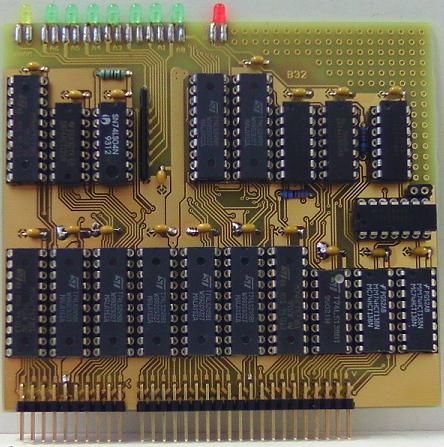
X45, experimental 6545 TTL implementation.
16 Bit video address output (instead of 14 Bit), transparent latches in the address output lines
for compensation of bus hold timing issues, and IIRC it was a three-state output.

Interlaced mode with some conceptual bugs, also sort of a horizontal scrolling mode where
one line of characters is 256 Bytes.

Image

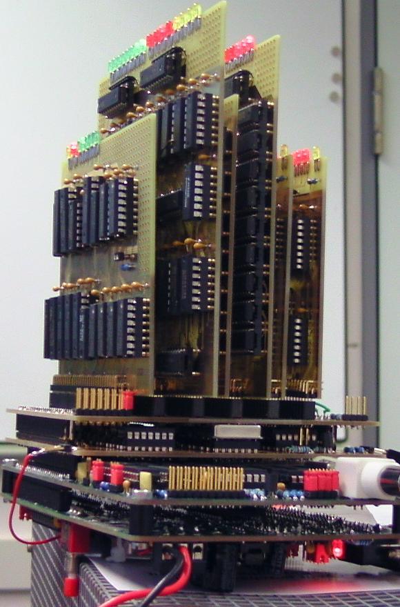
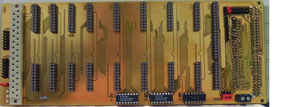
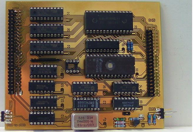
D45 demonstrator PCB (for generating a video signal) was plugged between the computer and the
X45 backplane.

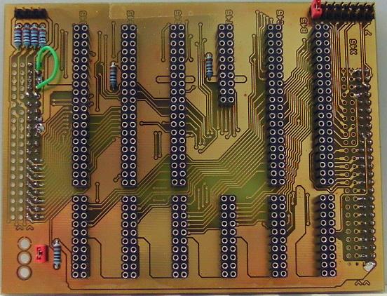
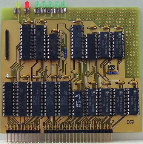
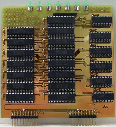
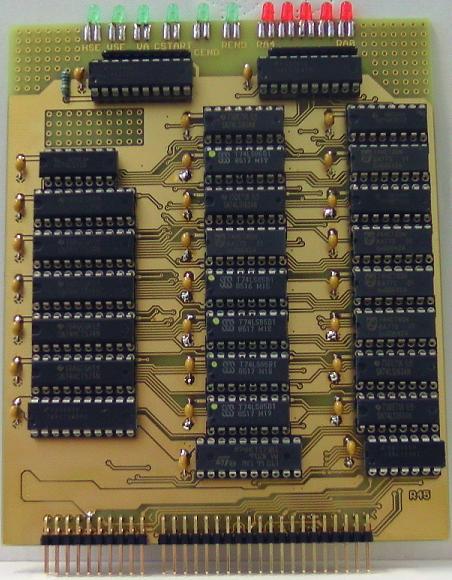
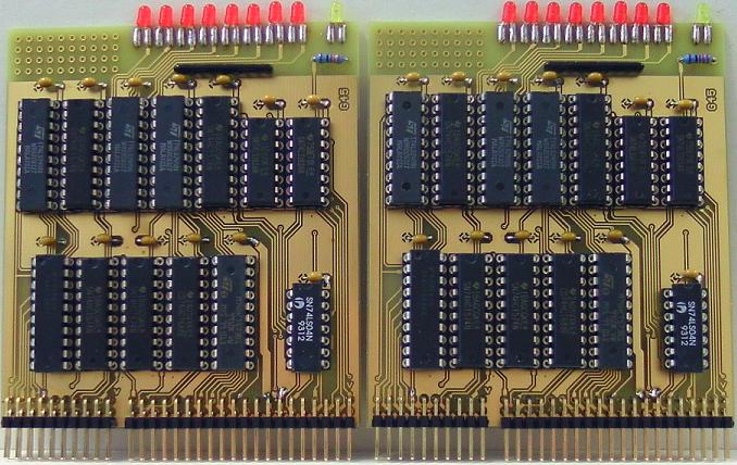
Plugged into the X45 backplane, we have:
1* B45, bus interface
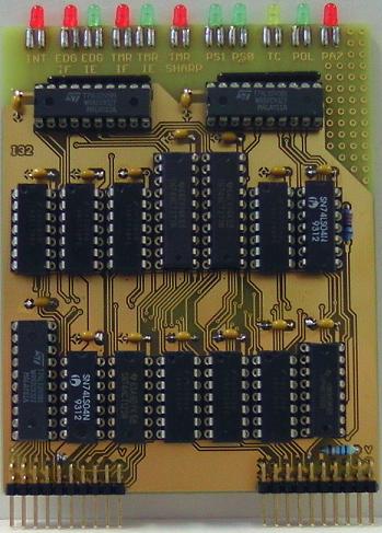
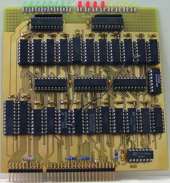
1* C45, the control module
1* T45, horizontal\vertical timing module
1* R45, raster timing module
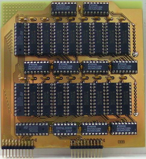
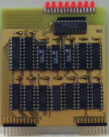
2* G45, two video address generator modules
User avatar
ttlworks
Posts: 1464
Joined: 09 Nov 2012
Contact:

Re: Experimental TTL implementation of the 6522

Post by ttlworks »

Let's start with D45, the demonstrator PCB containing the display RAM, the character ROM, the shift register etc.
80 characters per line (6502 has to run with a 2MHz clock generated by D45), monochrome analog video signal.

Image
d45_1.png
d45_2.png
d45_3.png
d45_4.png
d45_5.png
User avatar
ttlworks
Posts: 1464
Joined: 09 Nov 2012
Contact:

Re: Experimental TTL implementation of the 6522

Post by ttlworks »

The X45 backplane.
IIRC the little green wire was added for testing the light pen registers.

Image
x45_1.png
x45_2.png
x45_3.png
User avatar
ttlworks
Posts: 1464
Joined: 09 Nov 2012
Contact:

Re: Experimental TTL implementation of the 6522

Post by ttlworks »

B45, the bus interface to the 6502.

Image
b45_1.png
b45_2.png
b45_3.png
b45_4.png
b45_5.png
User avatar
ttlworks
Posts: 1464
Joined: 09 Nov 2012
Contact:

Re: Experimental TTL implementation of the 6522

Post by ttlworks »

T45, horizontal\vertical timing module

Image
t45_1.png
t45_2.png
t45_3.png
t45_4.png
t45_5.png
User avatar
ttlworks
Posts: 1464
Joined: 09 Nov 2012
Contact:

Re: Experimental TTL implementation of the 6522

Post by ttlworks »

R45, raster timing module

Image
r45_1.png
r45_2.png
r45_3.png
r45_4.png
r45_5.png
r45_6.png
User avatar
ttlworks
Posts: 1464
Joined: 09 Nov 2012
Contact:

Re: Experimental TTL implementation of the 6522

Post by ttlworks »

G45, video address generator module, two identical modules required

Image
g45_1.png
g45_2.png
g45_3.png
g45_4.png
g45_5.png
g45_6.png
User avatar
ttlworks
Posts: 1464
Joined: 09 Nov 2012
Contact:

Re: Experimental TTL implementation of the 6522

Post by ttlworks »

Now the last part:
C45, control module.

Unfinished work, has conceptual bugs, and you better design the whole thing again from scratch. I really mean it.

IIRC the intention was being able to run the video address generation circuitry at a higher frequency than the 6502 CPU,
with the idea in my backhead of porting the design to a CPLD someday, so I had decided to go with synchronous logic.

But this had bloated and complicated the logic design a lot, maybe it would better you go for another concept
like making creative use of RS flipflops at some places in the circuitry if you are trying to build something like that.

Image
c45_1.png
c45_2.png
c45_3.png
c45_4.png
c45_5.png
c45_6.png
c45_7.png
c45_8.png
c45_9.png
c45_10.png
Post Reply