Need people to check my SBC design.

For discussing the 65xx hardware itself or electronics projects.
Post Reply
Kellan
Posts: 5
Joined: 03 Dec 2018

Need people to check my SBC design.

Post by Kellan »

Recently I've started designing a PCB for my 65(C)02 project that I'm working on. I've never done anything of this type, so I want someone to check my design to make sure that it will work before I order the circuit board.

EasyEDA Link:
https://easyeda.com/kellanclark22/new-project2

Image:
Image
Last edited by Kellan on Sat Feb 09, 2019 2:18 pm, edited 4 times in total.
User avatar
GaBuZoMeu
Posts: 660
Joined: 01 Mar 2017
Location: North-Germany

Re: Need people to check my SBC design.

Post by GaBuZoMeu »

Hi Kellan,
I think the way you generate RBWE as you call it isn't how it should be. You need /WE to go inactive when PHI2 becomes 0. So use one free NAND (U7) to invert RWB then NAND this with PHI2. This should work. Further: connect all unused gate inputs to either VCC or GND, even when you do not need the gate at all. They might oscillate otherwise.
There is one LS (U8) - HC or AHC is better.
ALL your VCC connections are wrong. I think you know what I mean.
There is no pullup provided for an open /WE for your EEPROM. If the jumper P5 isn't set /WE would float!
There are no pullups for NMIB and IRQB - and you may add a pullup for VPB.

Don't know if I had overlooked something. I didn't check the pinning of any device.

Have fun.
Kellan
Posts: 5
Joined: 03 Dec 2018

Re: Need people to check my SBC design.

Post by Kellan »

Thank you.
1. I NANDed the clock and RWB to get a read enable, then inverted that to get the write.
2. I now have all the unused gate inputs connected to ground.
3. That's now fixed.
4. I cant believe I messed that up. I think they're good now.
5. I've never used a pullup resistor, but I think that's fixed.
6. I don't think I need pullups for IRQB and NMIB because they are controlled directly by the 65C22s, and since I'm using a WDC 65C02 I don't need a pullup according to the primer
Last edited by Kellan on Sat Feb 09, 2019 2:44 am, edited 1 time in total.
DerTrueForce
Posts: 483
Joined: 04 Jun 2016
Location: Australia

Re: Need people to check my SBC design.

Post by DerTrueForce »

Welcome to the world of 6502!

For future reference, when you post a schematic here, it's a good idea to post them in black and white. There are some people here who are colourblind, at least one of whom is very knowledgeable.

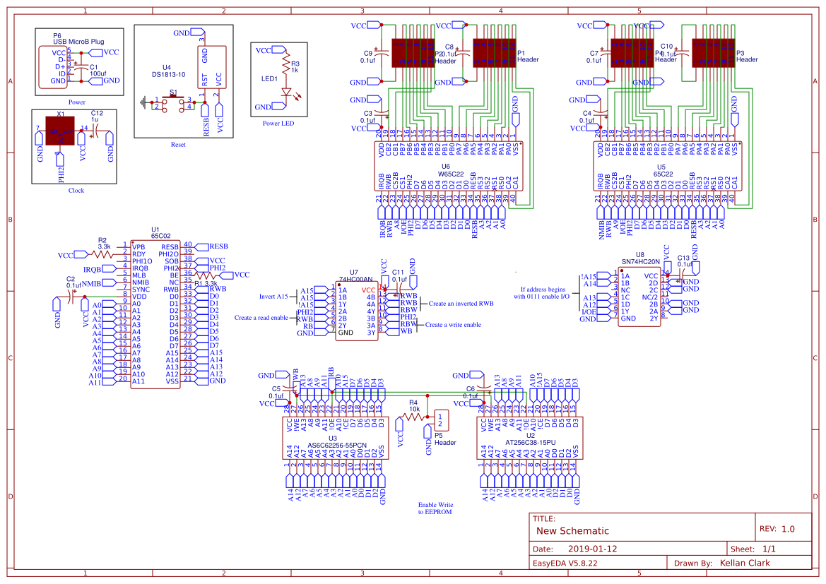
For the EEPROM write-enable jumper, I'd recommend using something like this(I use this in my own design):
Write-enable jumper.png
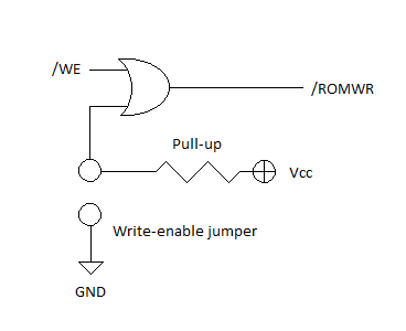
Write-enable jumper.png (3.55 KiB) Viewed 1011 times
This will ensure that your EEPROMs /WE input is deasserted(high) when the jumper is removed, and when inserted, /WE will be asserted when /WR is.
Your /RD and /WR generation isn't quite there. As it sits, you are generating /RD correctly(You've called it RWEB), but your /WR(RBWE) isn't correct, because it will be true whenever /RD is false, and that goes false when phase 2 is low. This will generate spurious writes(if those hit the EEPROM, your SBC will probably crash). I'd use a circuit like this, using gates from your 74HC00:
RD and WR generation.png
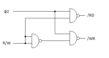
RD and WR generation.png (2.63 KiB) Viewed 1011 times
I also notice a complete lack of serial I/O. You may want a UART to make getting a display a bit easier(It's not necessary to it, though).
If you do choose to include a UART, I recommend staying away from the 65c51. It has a hardware bug that means it always reports as if it's completed transmitting a character, even when it's right in the middle of doing so. You can't use interrupts, and you can't poll it, so you have to time it somehow.
I would recommend the NXP 28L91 or 28L92 if you want a UART. You could also probably include a USB-to-UART chip there, as well, using the USB port that's already there.
Kellan
Posts: 5
Joined: 03 Dec 2018

Re: Need people to check my SBC design.

Post by Kellan »

Again, thank you. I just implemented those changes into the project.
My plan for the UART was to hook up one of my ports to a MAX 3100 and use that with an Arduino to connect to my computer kind of like this: https://coronax.wordpress.com/tag/max3100/
User avatar
drogon
Posts: 1671
Joined: 14 Feb 2018
Location: Scotland
Contact:

Re: Need people to check my SBC design.

Post by drogon »

Kellan wrote:
Again, thank you. I just implemented those changes into the project.
My plan for the UART was to hook up one of my ports to a MAX 3100 and use that with an Arduino to connect to my computer kind of like this: https://coronax.wordpress.com/tag/max3100/
Since you have 2 VIAs, then you could use one of the VIA ports as a bi-directional parallel interface directly to an Arduino, then the Arduino is your serial chip (and more, SPI, I2C if desired) - obviously a little more code to write, but at least the Arduino side is C.

(And hello, welcome :)

-Gordon
--
Gordon Henderson.
See my Ruby 6502 and 65816 SBC projects here: https://projects.drogon.net/ruby/
Post Reply