A simple 6502 SBC. Request for comments
-
GARTHWILSON

- Forum Moderator
- Posts: 8775
- Joined: 30 Aug 2002
- Location: Southern California
- Contact:
Re: A simple 6502 SBC. Request for comments
See Jeff Laughton's animated visualizations of timing margins. These excellent, drawn-to-scale (unlike most in data sheets) .gif's help understand what timings are constant and what varies with clock speed. Discussion about them is in the forum topic here.
http://WilsonMinesCo.com/ lots of 6502 resources
The "second front page" is http://wilsonminesco.com/links.html .
What's an additional VIA among friends, anyhow?
The "second front page" is http://wilsonminesco.com/links.html .
What's an additional VIA among friends, anyhow?

Re: A simple 6502 SBC. Request for comments
mdpye wrote:
Quote:
However, in the design of my POC V2's logic, I worked off the fall of Ø2.
From an engineering perspective, it's a matter of understanding what's a convention and what's a constraint.
FWIW even something as popular and long-lived as the BBC Micro isn't actually a very good design from this perspective. And Bil Herd has written several amusing stories about the state of play within Commodore - not good at all! But by trial and error and some luck and judgement, they made some very successful machines.
For a hobby project, built as a one-off, an empirical approach can take you a long way. Build a 100 to sell, and if you get 10 or 20 returns or field failures, that's going to be a lot of a grief.
Re: A simple 6502 SBC. Request for comments
Quote:
See Jeff Laughton's animated visualizations of timing margins. These excellent, drawn-to-scale (unlike most in data sheets) .gif's help understand what timings are constant and what varies with clock speed. Discussion about them is in the forum topic here.
I'm fairly clear on the *requirements*, what I'm more hazy on is the other side. If I'm told that a signal I want to latch will be stable x nanoseconds *after* a particular clock edge, what are good approaches to relating my latch enable to said clock? What is canonical good practice for introducing a precise deliberate delay in to a signal?
My guess from my experience with design in FPGAs would be to take it from the edge of a faster clock, counting edges if required. Or an deliberately introduced rc delay, although that feels a little... soft or imprecise to the software engineer in me (that's my background).
-
GARTHWILSON
- Forum Moderator
- Posts: 8775
- Joined: 30 Aug 2002
- Location: Southern California
- Contact:
Re: A simple 6502 SBC. Request for comments
mdpye wrote:
My guess from my experience with design in FPGAs would be to take it from the edge of a faster clock, counting edges if required. Or an deliberately introduced rc delay, although that feels a little... soft or imprecise to the software engineer in me (that's my background).
http://WilsonMinesCo.com/ lots of 6502 resources
The "second front page" is http://wilsonminesco.com/links.html .
What's an additional VIA among friends, anyhow?
The "second front page" is http://wilsonminesco.com/links.html .
What's an additional VIA among friends, anyhow?
Re: A simple 6502 SBC. Request for comments
What I'm getting from this, more or less, is that best case is use a cpld/fpga (where a bunch of counters are "cheap", and in the fpga case at least, clock multiplication is a common feature) or hope you can work from existing signal edges. I had a Google round commercial delay ICs, they look pretty... hardcore (a delay line needs 16+ pins?! Granted, many are for selecting the desired delay, but still...)
Re: A simple 6502 SBC. Request for comments
It might be that you don't need a delay: can you share your timing diagram? Personally I find it near-impossible to follow textual stories of what's going on, and words like 'gate' and 'latch' are potentially misleading if they mean different things to different people.
What I'm getting at is this: say, for example, the address bus from a CPU becomes valid about 30ns after the fall of Phi2. There's no need to capture this new value at that time, or any other time. If the bus stays static and valid until say 5ns after the following Phi2, then it will be valid for the entire time you need it.
Of course, your situation might be different.
Re: A simple 6502 SBC. Request for comments
So, I've been working hard when I can find the time, and I've come to the attached schematic (now presented in glorious black and white!)
It is considerably more involved that before - after looking more carefully at the serial handshaking, I decided to being the UART-USB interfaces on board.
Both the UART and RAM selects are now qualified with PHI2, with /OE driven by PHI1 (now properly generated from the clock circuit). The datasheet puts /OE as don't care during a write cycle.
The memory map and decoding has been re-done. It's possibly somewhat unconventional, but it seems pretty convenient to me, I could even place jumpers on the board to be able to reconfigure the memory map after fabrication. A15 on the RAM is wired to the bus to cover this eventuality.
The main motivation was the realisation that as this board has no provision for mass storage, I should perhaps be more generous with the addressable ROM so I can fit more code in to it.
All unused inputs are properly tied, and I've added a complement of decoupling caps, status LEDs and power in via a micro-usb port so that this design is also proposed as actually complete.
On the other hand, this is now way more than I might be able to test on a breadboard, and will be considerably larger on the PCB, so I'm more concerned than ever about potential bugs!
Speaking of board space, I am really starting to see the advantage of the PLCC package format. I have some PLCC EEPROMs, and they're less than half the size of the identical model DIP. On the other hand, ZIF sockets are hard to come by (for the ROM) and I already have the DIP parts for all the other major ICs. I'll be using SOIC for the 74 series ICs.
Edit: Schematic removed, because it was badly oriented. See download/file.php?id=5671 (comment below) for PDF.
Last edited by mdpye on Sat Nov 04, 2017 4:59 pm, edited 1 time in total.
-
Alarm Siren

- Posts: 363
- Joined: 25 Oct 2016
Re: A simple 6502 SBC. Request for comments
As I am unable to read sideways circuit schematics, I shall need to print this before I can give any meaningful feedback.
Want to design a PCB for your project? I strongly recommend KiCad. Its free, its multiplatform, and its easy to learn!
Also, I maintain KiCad libraries of Retro Computing and Arduino components you might find useful.
Also, I maintain KiCad libraries of Retro Computing and Arduino components you might find useful.
Re: A simple 6502 SBC. Request for comments
I was having some difficulty with my PDF generator, but sorted now.
Here's a correctly oriented copy, where I've also found better symbols for the RAM and ROM ICs (with logical, rather than physical schematic presentation)
Here's a correctly oriented copy, where I've also found better symbols for the RAM and ROM ICs (with logical, rather than physical schematic presentation)
- Attachments
-
- main.pdf
- (194.86 KiB) Downloaded 146 times
-
Alarm Siren
- Posts: 363
- Joined: 25 Oct 2016
Re: A simple 6502 SBC. Request for comments
Nope, that was still portrait by default. I have however just discovered that adobe has a rotate view function! woo!
Want to design a PCB for your project? I strongly recommend KiCad. Its free, its multiplatform, and its easy to learn!
Also, I maintain KiCad libraries of Retro Computing and Arduino components you might find useful.
Also, I maintain KiCad libraries of Retro Computing and Arduino components you might find useful.
-
Alarm Siren
- Posts: 363
- Joined: 25 Oct 2016
Re: A simple 6502 SBC. Request for comments
That is probably one of the more interesting uses for an '85 comparator i've seen, but I see no reason why it wouldn't work.
- CS_ROM is not gated by PHI2 like the other two are, I would suggest it probably should be. Also as it stands, it will be possible to write to the ROM chip - whilst this is fine, generally speaking the 28C' chips have specific requirements as to write cycles, its not like writing to RAM, so be careful you don't write to the ROM space when you don't mean to.
- I would recommend a bulk capacitor - say 10uF - on your system power input.
- If all inputs have weak internal pull-ups as stated, why do DCD and RI need to be pulled connected to Vcc?
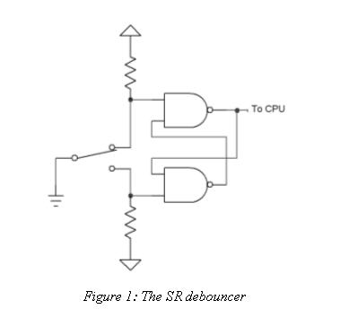
- I feel like your PHI1/2 generator: I would be concerned about the ability of that circuit to drive PHI2 properly, and PHI1 will be a little out of phase with PHI2 due to the delay in the second inverter. Rather than rolling your own crystal circuit, it'd be much easier to chuck in a oscillator can. If you use a 4MHz can and divide it down to 2MHz with a 74HC74, you get a 50% duty cycle clock and you get both PHI1 and PHI2 for free, with no phase difference between them. You can even use the second flip-flop in a 74HC74 package to implement debounce for a reset or NMI button.
- A suggestion: Have two USBs instead of three; one of them can do power and data. If you power it off a wall-wart then the data lines will do nothing anyway, and if you've plugged it into a PC chances are you want to power AND talk to it, so why use up two USB ports where one will do?
Want to design a PCB for your project? I strongly recommend KiCad. Its free, its multiplatform, and its easy to learn!
Also, I maintain KiCad libraries of Retro Computing and Arduino components you might find useful.
Also, I maintain KiCad libraries of Retro Computing and Arduino components you might find useful.
Re: A simple 6502 SBC. Request for comments
Quote:
CS_ROM is not gated by PHI2 like the other two are, I would suggest it probably should be. Also as it stands, it will be possible to write to the ROM chip - whilst this is fine, generally speaking the 28C' chips have specific requirements as to write cycles, its not like writing to RAM, so be careful you don't write to the ROM space when you don't mean to.
Quote:
I would recommend a bulk capacitor - say 10uF - on your system power input.
Quote:
If all inputs have weak internal pull-ups as stated, why do DCD and RI need to be pulled connected to Vcc?
Quote:
I feel like your PHI1/2 generator: I would be concerned about the ability of that circuit to drive PHI2 properly, and PHI1 will be a little out of phase with PHI2 due to the delay in the second inverter. Rather than rolling your own crystal circuit, it'd be much easier to chuck in a oscillator can. If you use a 4MHz can and divide it down to 2MHz with a 74HC74, you get a 50% duty cycle clock and you get both PHI1 and PHI2 for free, with no phase difference between them. You can even use the second flip-flop in a 74HC74 package to implement debounce for a reset or NMI button.
Quote:
A suggestion: Have two USBs instead of three; one of them can do power and data. If you power it off a wall-wart then the data lines will do nothing anyway, and if you've plugged it into a PC chances are you want to power AND talk to it, so why use up two USB ports where one will do?
Quote:
Other than that, it all looks good to me.
-
GARTHWILSON
- Forum Moderator
- Posts: 8775
- Joined: 30 Aug 2002
- Location: Southern California
- Contact:
Re: A simple 6502 SBC. Request for comments
I couldn't find where your GPIOs go (which the "weak" pull-ups are connected to), but if you truly want weak pull-ups, that would be more like a megohm, not 10K. I've had situations where I'd want something with 5 or 10 K of impedance to pull down to a solid logic '0' against a weak I/O, and they wouldn't be able to against a 10K.
http://WilsonMinesCo.com/ lots of 6502 resources
The "second front page" is http://wilsonminesco.com/links.html .
What's an additional VIA among friends, anyhow?
The "second front page" is http://wilsonminesco.com/links.html .
What's an additional VIA among friends, anyhow?
-
Alarm Siren
- Posts: 363
- Joined: 25 Oct 2016
Re: A simple 6502 SBC. Request for comments
mdpye wrote:
Oops, wiring R/W to the ROM /WE was entirely accidental, introduced when I switched the symbols in too much haste! Without the ability to write to the EEPROM in place, PHI2 gating of the /CS line shouldn't be necessary, right? The ROM is by far the slowest component to respond, and I wanted to give it as much time as possible, in case I am able to push the clock up a little on completion. It was mentioned that the UART will likely limit me to 3MHz, but even that would be a 50% increase in raw power, which would be neat...
mdpye wrote:
While a can sounds tempting, I do have a lot of bare crystals in a wide variety of frequencies already, so I would prefer to put them to use. But using a faster one and a flipflop would be a sensible move from the sounds of it. And debouncing using the spare unit is a great idea, thanks! That also reminds me that an NMI button for debugging lock-up crashes would be super useful.
 .
.mdpye wrote:
I thought about this. I guess I was a little worried about what the total power draw might be. I can use a decent wall wart, but laptop USB ports are - as I understand it - often somewhat under powered. That said, the unit doesn't have much in the way of useful IO besides a serial connection to a PC, so I will always be using it plugged in to one, and a single cable would be much more convenient!
Want to design a PCB for your project? I strongly recommend KiCad. Its free, its multiplatform, and its easy to learn!
Also, I maintain KiCad libraries of Retro Computing and Arduino components you might find useful.
Also, I maintain KiCad libraries of Retro Computing and Arduino components you might find useful.

Re: A simple 6502 SBC. Request for comments
Alarm Siren wrote:
If it is physically impossible to write to the ROM chip, and it will never become possible, then no, you shouldn't need to gate it by PHI2.
We all know that on each cycle there can be only one device driving the data bus, and that a gross violation of this rule will be a show-stopper. What's less well known is that the boundaries between cycles also present the threat of contention. Specifically, it's desirable that the previously active device complete the process of transitioning its outputs to high impedance before the incoming device exits high impedance and commences turning on. This seems almost impossible to guarantee. The enable and disable times of devices on the bus will vary -- and in some cases won't even be fully specified by the manufacturer.
The best -- and easiest -- solution is to observe the convention that nothing drives the data bus when PHI2 is low. (The 6502 chip itself observes this convention.) Thus the PHI2-low time provides a timing cushion during which each of the devices can promptly or lazily complete its part of the handover. Notice it's impossible to transfer data during this time anyway because the address bus isn't yet known to be valid. So there's little or no downside; the worst that can happen is you might need an extra gate.
Admittedly it is possible for a design to work despite transients of bus contention, but tolerating the problem is a decision with certain consequences regarding signal integrity and power consumption. It's also possible to "get lucky." For example you may experimentally find that even the minimum time taken for the (E)EPROM to begin driving the bus is longer than the maximum time taken for the preceding device to relinquish the bus. But the minimum time is often not specified by the manufacturer, in which case this -- like overclocking -- becomes a seat-of-the-pants practice rather than rigorous engineering.
In 1988 my 65C02 got six new registers and 44 new full-speed instructions!
https://laughtonelectronics.com/Arcana/ ... mmary.html
https://laughtonelectronics.com/Arcana/ ... mmary.html