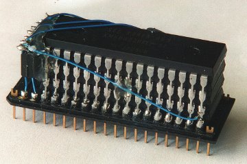
I have attached a logic diagram for the decoding logic I'm working on right now, and this is by far the most complex glue logic thing I've ever dreamt up so I'd like someone to check it over, please, and of course as always all comments/suggestions/rants are welcome.
--------
I'll explain what I'm trying to achieve...
Basic Memory Map:
Code: Select all
E000-FFFF   ROM
C000-DFFF   I/O (subdivided into 8x1KiB)
8000-BFFF   Banked RAM
0000-7FFF Standard RAMI/O is 8KiB subdivided into 1KiB blocks, each one assigned to an IO device using the !IOCS0, !IOCS1 (etc) lines. I don't have any I/O devices that need that much space, but it doing it this way needed less glue chips. There are three devices here (though obviously up to 8 could be used in theory): a VIA, a UART and a Bank Register (we'll get to that).
Standard RAM: Completely bog-standard 32KiB of RAM, being the lowest quarter of a 128KiB RAM chip.
Banked RAM: OK, so, the idea is there's a register at $C800 which can be read and written, implemented with a '574 and a '245. The lowest three bits of this register are substituted for the CPU's A16, A15 and A14 lines (by means of a '157 multiplexer) when accessing, what is from the CPU's point of view, the address range 8000-DFFF. The upshot of this is that this range, using the bank register, allows you to access the entire 128KiB of RAM - including mirroring the 32KiB Standard RAM. The downside is needing to fiddle with a bank register and that you can only do so through a 16KiB "window".
For clarification: Yes, I did mean A16 then, and I do know that's not an address line that exists on the CPU - it does however exist on the RAM chip. When not accessing banked RAM, the multiplexer supplies a zero to this line. I could have made the bank register Write Only, but I decided to make it readable so that interrupt code / subroutines can save/restore it.
-----
Thanks in advance.