6502.org Forum  Projects  Code  Documents  Tools  Forum
It is currently Sat Nov 23, 2024 9:02 am

All times are UTC


Post new topic Reply to topic  [ 57 posts ]  Go to page 1, 2, 3, 4  Next
Author Message
 Post subject: Monster Decoding Logic
PostPosted: Tue Sep 26, 2017 1:25 am 
Offline
User avatar

Joined: Tue Oct 25, 2016 8:56 pm
Posts: 362
Hello!

I have attached a logic diagram for the decoding logic I'm working on right now, and this is by far the most complex glue logic thing I've ever dreamt up so I'd like someone to check it over, please, and of course as always all comments/suggestions/rants are welcome.

--------

I'll explain what I'm trying to achieve...

Basic Memory Map:
Code:
E000-FFFF   ROM
C000-DFFF   I/O (subdivided into 8x1KiB)
8000-BFFF   Banked RAM
0000-7FFF   Standard RAM


ROM is fairly self-explantory: the upper 8KiB selects the 8KiB ROM chip using !ROMCS.

I/O is 8KiB subdivided into 1KiB blocks, each one assigned to an IO device using the !IOCS0, !IOCS1 (etc) lines. I don't have any I/O devices that need that much space, but it doing it this way needed less glue chips. There are three devices here (though obviously up to 8 could be used in theory): a VIA, a UART and a Bank Register (we'll get to that).

Standard RAM: Completely bog-standard 32KiB of RAM, being the lowest quarter of a 128KiB RAM chip.

Banked RAM: OK, so, the idea is there's a register at $C800 which can be read and written, implemented with a '574 and a '245. The lowest three bits of this register are substituted for the CPU's A16, A15 and A14 lines (by means of a '157 multiplexer) when accessing, what is from the CPU's point of view, the address range 8000-DFFF. The upshot of this is that this range, using the bank register, allows you to access the entire 128KiB of RAM - including mirroring the 32KiB Standard RAM. The downside is needing to fiddle with a bank register and that you can only do so through a 16KiB "window".

For clarification: Yes, I did mean A16 then, and I do know that's not an address line that exists on the CPU - it does however exist on the RAM chip. When not accessing banked RAM, the multiplexer supplies a zero to this line. I could have made the bank register Write Only, but I decided to make it readable so that interrupt code / subroutines can save/restore it.

-----

Thanks in advance.

Attachments:
File comment: NimbotCalc Logic Diagram
Logic.png
Logic.png [ 14.25 KiB | Viewed 2531 times ]

_________________
Want to design a PCB for your project? I strongly recommend KiCad. Its free, its multiplatform, and its easy to learn!
Also, I maintain KiCad libraries of Retro Computing and Arduino components you might find useful.


Last edited by Alarm Siren on Tue Sep 26, 2017 3:52 pm, edited 1 time in total.
Top
 Profile  
Reply with quote  
PostPosted: Tue Sep 26, 2017 4:21 am 
Offline
User avatar

Joined: Fri Dec 11, 2009 3:50 pm
Posts: 3367
Location: Ontario, Canada
A few thoughts come to mind. For example, a 65c816 could address extra memory far more effectively. But I assume the goal is to use a 'C02, and intentionally do things the hard way! :)

Regarding the I/O port that supplies the high address bits, rather than building your own out of the '574 and '245, have you considered adding an extra 65c22 to the system? That'd give you the I/O port you need, plus a lot more. And it eliminates some of the complexity in the glue logic.

Along the same lines, you could eliminate the complexity of the '157 multiplexer if you simply used two separate RAM chips attached to the two separate address sources. Depending how it's done, you might end up with a larger total amount of RAM. This might raise costs, though. Do you need to worry about that? "One-off" experiments tend to be less cost-sensitive than something intended for production.

-- Jeff

_________________
In 1988 my 65C02 got six new registers and 44 new full-speed instructions!
https://laughtonelectronics.com/Arcana/ ... mmary.html


Top
 Profile  
Reply with quote  
PostPosted: Tue Sep 26, 2017 10:42 am 
Offline
User avatar

Joined: Tue Oct 25, 2016 8:56 pm
Posts: 362
Quote:
For example, a 65c816 could address extra memory far more effectively. But I assume the goal is to use a 'C02, and intentionally do things the hard way! :)


Unfortunately, I'm not mentally ready for a 65816 yet. I totally understand the benefits and one day, I'm sure I'll make the jump and never look back. Today is not that day, it still gives me the heeby-jeebies! :(

Quote:
Regarding the I/O port that supplies the high address bits, rather than building your own out of the '574 and '245, have you considered adding an extra 65c22 to the system? That'd give you the I/O port you need, plus a lot more. And it eliminates some of the complexity in the glue logic.


No, I had not considered using another VIA. as you say, that would significantly simplify the circuit overall, I think overall it'd be a tad more expensive than the chips it replaces but not by much. On the other hand, I have no particular need for any of the other extra functionality it would provide over a single VIA.

Quote:
Along the same lines, you could eliminate the complexity of the '157 multiplexer if you simply used two separate RAM chips attached to the two separate address sources. Depending how it's done, you might end up with a larger total amount of RAM. This might raise costs, though. Do you need to worry about that? "One-off" experiments tend to be less cost-sensitive than something intended for production.


Again, quite sensible idea. That would actually give more RAM overall as you say - the 32KiB standard would remain, and then the extended ram would window into an entirely seperate 128KiB - giving 160 in total. Does add a RAM chip to the system, which aren't small, but also not the end of the world. Cost of parts isn't so much a problem as the size of the PCB they've got to sit on. I shall give this suggestion consideration, it really does come down to board space more than anything else.


The reason for all this hoop-jumping was that I find it distasteful to not make full use of all the hardware available to me. For my original memory layout, I was resigned to the fact that I would be 'wasting' 16K of a 64K memory chip - no one makes a 48K RAM chip! However, having found you can't actually seem to buy 64K SRAM chips and it jumps straight up to 128K, I didn't want to waste over half of the RAM I paid for. Also, setting a challenge for one's self is fun.

_________________
Want to design a PCB for your project? I strongly recommend KiCad. Its free, its multiplatform, and its easy to learn!
Also, I maintain KiCad libraries of Retro Computing and Arduino components you might find useful.


Last edited by Alarm Siren on Tue Sep 26, 2017 1:27 pm, edited 1 time in total.

Top
 Profile  
Reply with quote  
PostPosted: Tue Sep 26, 2017 1:24 pm 
Offline
User avatar

Joined: Tue Oct 25, 2016 8:56 pm
Posts: 362
Taking on board Jeff's suggestions has massive simplified the design (see attached).

Broadly speaking it maintains the same basic memory map, but the total amount of accessible RAM will now be 160KiB across a 128K and a 32K chip. I was reserving Port A of the VIA already in the system for a user GPIO port, but an extra 112KB of RAM is probably worth sacrificing three GPIO pins. User software should only be accessing the VIA through the BIOS API anyway, so they can still have 5 GPIOs without risk of stepping on the bank bits.

I don't actually need to subdivide the I/O space into 1K blocks; I've only got two I/O devices so 4K blocks will do. A hypothetical future version of the board with more I/O devices can simply further subdivide the 4K blocks without stepping on backwards compatibility.

Reduction from roughly 9 chips of glue logic to 3 plus a NOT gate, though I am adding an extra RAM chip by doing so.


Attachments:
File comment: Logic Diagram v2
Logic.png
Logic.png [ 9.68 KiB | Viewed 2478 times ]

_________________
Want to design a PCB for your project? I strongly recommend KiCad. Its free, its multiplatform, and its easy to learn!
Also, I maintain KiCad libraries of Retro Computing and Arduino components you might find useful.
Top
 Profile  
Reply with quote  
PostPosted: Tue Sep 26, 2017 2:44 pm 
Offline
User avatar

Joined: Fri Dec 11, 2009 3:50 pm
Posts: 3367
Location: Ontario, Canada
Ooo, that looks better. :) As for the '816, I'll note in passing that it doesn't force you to jump into the deep end of the pool; it has mode bits which turn off its 816-ness by default. Later you can progressively enable those bits one by one and wade into the pool at your own pace.

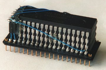
On the topic of board space, have you considered piggybacking the memory chips? Two (or more!) chips get soldered on atop the other, with almost all the leads connected in parallel. Typically it's only the /CE pin which requires a separate "flying" lead, but in your case a few of the high address lines would also need separate treatment.

Piggybacking looks a bit funny, but the saving in board space is very compelling. The photo shows eight RAM's in the space of four. .6" DIP's with .1" lead pitch are the easiest to piggyback, but .4" SOJ packages with .050" lead pitch are eligible, too. You just need to uncurl the J-leads first.


Attachments:
KK 0791ram fr.jpg
KK 0791ram fr.jpg [ 110.93 KiB | Viewed 2469 times ]

_________________
In 1988 my 65C02 got six new registers and 44 new full-speed instructions!
https://laughtonelectronics.com/Arcana/ ... mmary.html
Top
 Profile  
Reply with quote  
PostPosted: Tue Sep 26, 2017 3:49 pm 
Offline
User avatar

Joined: Thu Dec 11, 2008 1:28 pm
Posts: 10986
Location: England
I like this memory map! I think there might be a typo: DFFF for BFFF?


Top
 Profile  
Reply with quote  
PostPosted: Tue Sep 26, 2017 3:52 pm 
Offline
User avatar

Joined: Tue Oct 25, 2016 8:56 pm
Posts: 362
Quite right. Fixed it.

_________________
Want to design a PCB for your project? I strongly recommend KiCad. Its free, its multiplatform, and its easy to learn!
Also, I maintain KiCad libraries of Retro Computing and Arduino components you might find useful.


Top
 Profile  
Reply with quote  
PostPosted: Tue Sep 26, 2017 4:09 pm 
Offline
User avatar

Joined: Thu Dec 11, 2008 1:28 pm
Posts: 10986
Location: England
Nice being able to use a few bits from the VIA you already have.


Top
 Profile  
Reply with quote  
PostPosted: Tue Sep 26, 2017 4:15 pm 
Offline
User avatar

Joined: Fri Dec 11, 2009 3:50 pm
Posts: 3367
Location: Ontario, Canada
Here's some further noodling [with the booboo fixed, now :oops: ]. And there's another change which I didn't bother drawing. IIRC the 128K RAM has two CS inputs, and using both (straight from A15 & A14) would mean the '139 upper section isn't required to select that RAM. Likewise that '139 upper section isn't required to select the 32K RAM. So, I suggest you delete that upper section. Then the lower section can be replaced with a '138, accepting A15 & A14 on the appropriate enable inputs. There's no increase in functionality, but propagation delay is reduced (compared to cascading two sections of a '139).

Quote:
I didn't want to waste over half of the RAM I paid for.
I fully understand this feeling, but nevertheless there's a clear advantage if you want to piggyback. It's somewhat easier to attach together two 128K chips than to attach a 128K chip and a 32K chip. Instead of thinking about the percentage of capacity you're wasting, maybe the compromise will be more palatable if you simply look at the cost difference. I expect 128K is only a little more expensive than 32K -- and practical considerations may justify that small extra expense.


Attachments:
Logic with suggested mod's.png
Logic with suggested mod's.png [ 15.12 KiB | Viewed 2445 times ]

_________________
In 1988 my 65C02 got six new registers and 44 new full-speed instructions!
https://laughtonelectronics.com/Arcana/ ... mmary.html


Last edited by Dr Jefyll on Tue Sep 26, 2017 5:24 pm, edited 1 time in total.
Top
 Profile  
Reply with quote  
PostPosted: Tue Sep 26, 2017 5:21 pm 
Offline
User avatar

Joined: Tue Oct 25, 2016 8:56 pm
Posts: 362
Dr Jefyll wrote:
Oops, and a booboo with that inverter. Stand by while I edit the diagram.


By all means fix the diagram, but I already spotted and corrected for that mistake :D

_________________
Want to design a PCB for your project? I strongly recommend KiCad. Its free, its multiplatform, and its easy to learn!
Also, I maintain KiCad libraries of Retro Computing and Arduino components you might find useful.


Top
 Profile  
Reply with quote  
PostPosted: Tue Sep 26, 2017 5:25 pm 
Offline
User avatar

Joined: Fri Dec 11, 2009 3:50 pm
Posts: 3367
Location: Ontario, Canada
You're fast!

[Edit: Dang, that was supposed to be a PM but I hit the wrong button. One booboo follows another! But no harm done, I guess.]

_________________
In 1988 my 65C02 got six new registers and 44 new full-speed instructions!
https://laughtonelectronics.com/Arcana/ ... mmary.html


Top
 Profile  
Reply with quote  
PostPosted: Tue Sep 26, 2017 6:07 pm 
Offline
User avatar

Joined: Tue Oct 25, 2016 8:56 pm
Posts: 362
Here we go,

Its just as well, as I was doing this I suddenly remembered (with an acompanying facepalm) there is a third I/O device - the screen! Luckily this has 4 I/O spaces 'so its all good.

I very much like the look of this. Its down to three chips and three inverters, so I think its safe to say this monster has been tamed. I doubt we can make it much simpler..... *waits for Jeff to pull another rabbit out of his hat*


Attachments:
Logic.png
Logic.png [ 10.57 KiB | Viewed 2439 times ]

_________________
Want to design a PCB for your project? I strongly recommend KiCad. Its free, its multiplatform, and its easy to learn!
Also, I maintain KiCad libraries of Retro Computing and Arduino components you might find useful.
Top
 Profile  
Reply with quote  
PostPosted: Tue Sep 26, 2017 6:28 pm 
Offline
User avatar

Joined: Fri Aug 30, 2002 1:09 am
Posts: 8545
Location: Southern California
Dr Jefyll wrote:
As for the '816, I'll note in passing that it doesn't force you to jump into the deep end of the pool; it has mode bits which turn off its 816-ness by default. Later you can progressively enable those bits one by one and wade into the pool at your own pace.

Yep, and it will be easier both in hardware and in software.

Quote:
On the topic of board space, have you considered piggybacking the memory chips? Two (or more!) chips get soldered on atop the other, with almost all the leads connected in parallel. Typically it's only the /CE pin which requires a separate "flying" lead, but in your case a few of the high address lines would also need separate treatment.

Piggybacking looks a bit funny, but the saving in board space is very compelling. The photo shows eight RAM's in the space of four. .6" DIP's with .1" lead pitch are the easiest to piggyback, but .4" SOJ packages with .050" lead pitch are eligible, too. You just need to uncurl the J-leads first.

Here's one of my first attempts at getting denser thru-hole RAM, 2MB, using four 512KB SRAMs, stacked:
Image
(The picture is from the chapter in the 6502 primer, "Getting More On a Board."

_________________
http://WilsonMinesCo.com/ lots of 6502 resources
The "second front page" is http://wilsonminesco.com/links.html .
What's an additional VIA among friends, anyhow?


Top
 Profile  
Reply with quote  
PostPosted: Tue Sep 26, 2017 6:43 pm 
Offline
User avatar

Joined: Fri Dec 11, 2009 3:50 pm
Posts: 3367
Location: Ontario, Canada
Alarm Siren wrote:
Its down to three chips and three inverters [... ] I doubt we can make it much simpler.....
Not much simpler, no. At first I thought we could dispense with that inverter on the input of the '138, but that idea turns out to be a dead end (despite a '138's otherwise versatile complement of active-high and active-low enable inputs).

However, the 4-input AND can be deleted. Instead, /CE for the EEPROM can be generated by a 3-input NAND fed by A15-13. A single 14-pin DIP holds three 3-input NAND's, so there are two left over... which can function as inverters. So, we now require three chips and just one inverter. Maybe you'd like to eliminate that last inverter by just using a transistor to complement Reset?

_________________
In 1988 my 65C02 got six new registers and 44 new full-speed instructions!
https://laughtonelectronics.com/Arcana/ ... mmary.html


Top
 Profile  
Reply with quote  
PostPosted: Tue Sep 26, 2017 6:54 pm 
Offline
User avatar

Joined: Wed Mar 01, 2017 8:54 pm
Posts: 660
Location: North-Germany
You are using PHI0 - sure?


Top
 Profile  
Reply with quote  
Display posts from previous:  Sort by  
Post new topic Reply to topic  [ 57 posts ]  Go to page 1, 2, 3, 4  Next

All times are UTC


Who is online

Users browsing this forum: No registered users and 37 guests


You cannot post new topics in this forum
You cannot reply to topics in this forum
You cannot edit your posts in this forum
You cannot delete your posts in this forum
You cannot post attachments in this forum

Search for:
Jump to: