Welcome, drfiemost

Ed and others here have some degree of expertise to offer, but you may have to explain some details about
what the SID chip does before we can grasp
how it's done (or how its behavior can be modeled). I did check the
MOS Technology SID page on wikipedia, and the links there led me to the Block Diagram shown below (on
http://www.waitingforfriday.com/index.p ... _Datasheet )
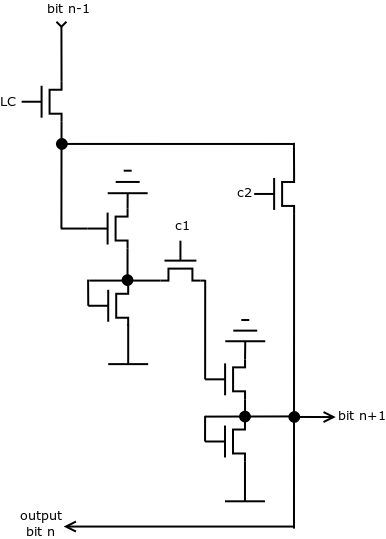
the noise waveform is generated taking the output of eight selected bits from a 23 bit Fibonacci LFSR (there are actually 24 bits on chip but the last one is unused). The register is clocked when bit 19 of the oscillator goes high [...] Each bit is formed by two inverters feeding each other through the gates c1 and c2, while the gate LC controls the shifting.
I think I'm clear on this part but corrections are welcome, of course. I expect that c1 and c2 are never active simultaneously -- instead, they takes turns. When active, c1 causes the output of the upper inverter to be applied to the input of the lower inverter. Likewise, c2 when active applies the output of the lower one to the upper. At the system clock rate Φ2 the cycle repeats -- c1, c2, c1, c2, c1, c2 etc. This activity continues at all times when the shift register isn't shifting -- it's a holding pattern, one which produces no change in the inverter outputs because we're just passing the existing value back and forth (inverting it twice, but that's incidental). In order for a shift to occur, LC becomes active during one of the the time-slots normally belonging to c2 (and c2 is inactive, missing its turn). For example, the sequence c1, c2, c1, c2, c1,
LC, c1, c2... means one shift has occurred.
Edit: in the following post, Dieter suggests a slightly different switching pattern which would also work; ie: c1, c2, c1, c2,
c1 as well as LC, c2... Of the two patterns, Dieter's is more likely what the SID does.
Forgive me if this is too much detail. I'm trying to provide the background for Ed's remark. It would be abnormal for c2 and LC to go active simultaneously, but if they did then the result will be an AND, as he noted. The output of the lower inverter will be ANDed with what's coming in from bit n-1, and the result gets input to the upper inverter.
It's maybe best if I sign off for now. Perhaps you can explain your remark, "when combining the noise with other waveforms the output bits may be driven low locking up the LFSR at zero." To me, the Block Diagram suggests that "combining the noise with other waveforms" is something entirely external to the shift registers (one of which is included in each Tone Oscillator/Waveform Generator). Maybe you can clarify what the interaction is.
cheers,
Jeff
Edit: Here's the LFSR bit drawn in a slightly different style.