6502.org Forum  Projects  Code  Documents  Tools  Forum
It is currently Fri Nov 22, 2024 5:24 am

All times are UTC


Post new topic Reply to topic  [ 164 posts ]  Go to page 1, 2, 3, 4, 5 ... 11  Next
Author Message
 Post subject: Understanding the SID
PostPosted: Wed Jun 08, 2016 4:06 pm 
Offline
User avatar

Joined: Tue Jun 07, 2016 4:34 pm
Posts: 53
This is my attempt at reverse-engineering (parts of) the SID chip from the schematics available at http://oms.wmhost.com/misc/. I'm not a hardware guy so support from experts is needed :P.
The results of this research wil be used to improve the open-source reSID emulation and will be put online at the libsidplayfp project wiki.

Let's start with the noise generator. As already known the noise waveform is generated taking the output of eight selected bits from a 23 bit Fibonacci LFSR (there are actually 24 bits on chip but the last one is unused). The register is clocked when bit 19 of the oscillator goes high and has taps at 17 and 22. The register can be reset using the test bit.

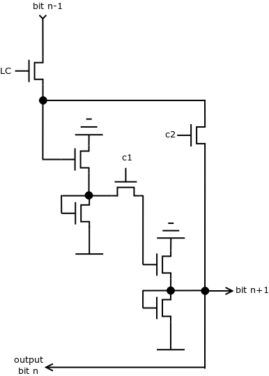
Each bit is formed by two inverters feeding each other through the gates c1 and c2, while the gate LC controls the shifting. The output from bits 0, 2, 5, 9, 11, 14, 18 and 20 is sent to the waveform selector. Here's the first two bits from the vectorized IC and the transistor scheme for a single bit:
Image

So the first question is:
when combining the noise with other waveforms the output bits may be driven low locking up the LFSR at zero. My understanding is that this happens only when when the gate LC is opened, during shifting or when the test bit is set, as the output bits are then feeded into the next ones (this seems to be confirmed by empirical tests, see VICE's bug 746). Is this correct? In other words, is it safe to assume that when a bit output (e.g. Noise 0 in the above picture) is grounded the bit itself is not written into?


Top
 Profile  
Reply with quote  
PostPosted: Wed Jun 08, 2016 5:30 pm 
Offline
User avatar

Joined: Thu Dec 11, 2008 1:28 pm
Posts: 10985
Location: England
Generally, NMOS digital circuits work like open-collector - every logic gate has a passive pullup, so if you tie two logic gate outputs together, you get the AND of the result. The pullups end up in parallel, and the pulldown trees are also in parallel, so if either pulls down the output will be zero.

In this case, here's what I'd expect: the pass gate LC acts somewhat like the feedback transistor clocked by c2. If the output is held low and c2 goes high, then the storage node which is the input of the first inverter will be discharged. On the next c1 the new value will be clocked into the next storage node (inverted of course) and the output of that inverter, and therefore the flop, will be a zero.

So, I would say if the output is grounded while c2 is high, and if LC doesn't replace the overwritten value with the correct one, then yes, the value will be changed.

But it seems empirical results say otherwise! So perhaps LC is in play to repair the discharged value?

Perhaps you could show some diagrammatic waveforms as to how c1, c2 and LC change?


Top
 Profile  
Reply with quote  
PostPosted: Wed Jun 08, 2016 11:36 pm 
Offline
User avatar

Joined: Fri Dec 11, 2009 3:50 pm
Posts: 3367
Location: Ontario, Canada
Welcome, drfiemost :)

Ed and others here have some degree of expertise to offer, but you may have to explain some details about what the SID chip does before we can grasp how it's done (or how its behavior can be modeled). I did check the MOS Technology SID page on wikipedia, and the links there led me to the Block Diagram shown below (on http://www.waitingforfriday.com/index.p ... _Datasheet )
Attachment:
SID_Block_Diagram.PNG
SID_Block_Diagram.PNG [ 51.49 KiB | Viewed 42045 times ]

drfiemost wrote:
the noise waveform is generated taking the output of eight selected bits from a 23 bit Fibonacci LFSR (there are actually 24 bits on chip but the last one is unused). The register is clocked when bit 19 of the oscillator goes high [...] Each bit is formed by two inverters feeding each other through the gates c1 and c2, while the gate LC controls the shifting.

I think I'm clear on this part but corrections are welcome, of course. I expect that c1 and c2 are never active simultaneously -- instead, they takes turns. When active, c1 causes the output of the upper inverter to be applied to the input of the lower inverter. Likewise, c2 when active applies the output of the lower one to the upper. At the system clock rate Φ2 the cycle repeats -- c1, c2, c1, c2, c1, c2 etc. This activity continues at all times when the shift register isn't shifting -- it's a holding pattern, one which produces no change in the inverter outputs because we're just passing the existing value back and forth (inverting it twice, but that's incidental). In order for a shift to occur, LC becomes active during one of the the time-slots normally belonging to c2 (and c2 is inactive, missing its turn). For example, the sequence c1, c2, c1, c2, c1, LC, c1, c2... means one shift has occurred.

Edit: in the following post, Dieter suggests a slightly different switching pattern which would also work; ie: c1, c2, c1, c2, c1 as well as LC, c2... Of the two patterns, Dieter's is more likely what the SID does.

Forgive me if this is too much detail. I'm trying to provide the background for Ed's remark. It would be abnormal for c2 and LC to go active simultaneously, but if they did then the result will be an AND, as he noted. The output of the lower inverter will be ANDed with what's coming in from bit n-1, and the result gets input to the upper inverter.

It's maybe best if I sign off for now. Perhaps you can explain your remark, "when combining the noise with other waveforms the output bits may be driven low locking up the LFSR at zero." To me, the Block Diagram suggests that "combining the noise with other waveforms" is something entirely external to the shift registers (one of which is included in each Tone Oscillator/Waveform Generator). Maybe you can clarify what the interaction is.

cheers,
Jeff

Edit: Here's the LFSR bit drawn in a slightly different style.

Attachments:
LFSR_bit redrawn.png
LFSR_bit redrawn.png [ 8.17 KiB | Viewed 42031 times ]

_________________
In 1988 my 65C02 got six new registers and 44 new full-speed instructions!
https://laughtonelectronics.com/Arcana/ ... mmary.html


Last edited by Dr Jefyll on Thu Jun 09, 2016 1:50 pm, edited 1 time in total.
Top
 Profile  
Reply with quote  
PostPosted: Thu Jun 09, 2016 7:11 am 
Offline
User avatar

Joined: Fri Nov 09, 2012 5:54 pm
Posts: 1431
Jeff, thanks for the picture.

I'm no expert when it comes to reverse engineering chips,
but I tried to draw your LFSR bit picture slightly different:

Attachment:
ff1.png
ff1.png [ 13.47 KiB | Viewed 42021 times ]


To me, this looks like a half_static one bit "storage cell",
similar to how the registers are implemented in the NMOS 6502.

If the LC and C1 switches are closed and the C2 switch is open,
the cell is cleared/set by discharging/charging the capacitors.

If the C2 switch is closed, and the LC and C1 switches are open,
the "storage cell" just holds the data...
unless a transistor not shown in the picture ties the output to GND,
of course.

Attachment:
ff2.png
ff2.png [ 13.77 KiB | Viewed 42021 times ]


Top
 Profile  
Reply with quote  
PostPosted: Thu Jun 09, 2016 9:11 am 
Offline
User avatar

Joined: Thu Dec 11, 2008 1:28 pm
Posts: 10985
Location: England
(Thanks for the redrawn schematics, Jeff and Dieter)

Indeed, it's a recirculating master-slave flop made from two dynamic latches. The S register of the 6502 is implemented like this. Notably, the X and Y registers are not: they lack the clocked feedback. I think that saves a little space. As a consequence, of the three, only S can be read and written in the same clock cycle.

The question is perhaps what the output multiplexing looks like. If more than one of the sources is selected, are the outputs in effect (resistively) shorted together? If so, what happens next may have something of an analogue nature - if one of the other sources is driving low, it has some effective resistance in pulling down the output of the LFSR. (In my first response I was thinking of transistors as switches, but they are more like voltage-controlled resistors.)

I think part of the fascination of the SID and the great difficulty in reproducing it is that it's not entirely a digital chip, and in exploring unanticipated ways of using it, even more so. I gather there are different revisions of SID which sound different to the trained ear - which means you even have to choose which revision you intend to emulate.


Top
 Profile  
Reply with quote  
PostPosted: Thu Jun 09, 2016 11:02 am 
Offline
User avatar

Joined: Tue Jun 07, 2016 4:34 pm
Posts: 53
You're right, I'm dealing with the chip since a while now so I may give some things for granted, I'll add more details as needed.

The SID can generate four kind of waveforms: Triangle, Sawtooth, Pulse and Noise. The first three come from a 24 bit phase accumulating oscillator while the latter from the shift register. It is possible to select more than one waveform at the same time producing weird sounds, due to the fact that the output of the waveforms are connected toghether causing an analogue effect which tends to pull down many of the bits.
Here is the output multiplexing part for the 6581:

Attachment:
Combined_waveforms.png
Combined_waveforms.png [ 15.87 KiB | Viewed 42000 times ]

where the Tri, Saw, Pul and Noi transistors are the waveform selectors and TRx, SWx, PLx and NSx are the outputs of the waveform generators. The triangle is generated by passing the Sawtooth through an xor logic, more on this in a future post.

As you can see the triangle selector interconnects adjacent bits and the pulse selector connects all the bits to the same line.
So when the noise waveform is selected along with others the LFSR bits may be driven low by the other waveform output.

In the next post I'll show the LFSR clock generator.


Top
 Profile  
Reply with quote  
PostPosted: Thu Jun 09, 2016 1:07 pm 
Offline

Joined: Wed Apr 27, 2016 2:15 pm
Posts: 141
Location: South Africa
Very interesting project. I am looking forward to your future posts!


Top
 Profile  
Reply with quote  
PostPosted: Thu Jun 09, 2016 1:27 pm 
Offline
User avatar

Joined: Fri Nov 09, 2012 5:54 pm
Posts: 1431
Since not everybody around here might be familiar with the concept of a NCO
(numerically controlled oscillator),
I felt a need to add some short background.

For generating a sine wave, for instance it could look like this:

Attachment:
dds.png
dds.png [ 46.33 KiB | Viewed 41984 times ]


We have a 24 Bit phase accumulator, that's just a register.

A 16 Bit "tuning word" (constant) is added to the phase accumulator
at a given frequency, let's say PHI2.

The time period between the phase accumulator overflows gives us
the frequency of the output signal.

To generate a neat signal, we just take the 12 uppermost bits
of the phase accumulator, what would give us (in the best case)
a sawtooth (like if we would be reading a 6522 timer or such).

For generating a sine wave, we use those 12 bits as address lines
for a ROM which contains a lookup table feeding a DAC with
the data outputs, and that's it.

So much for the theory.

;---

Unfortunately, there wasn't enough space on the silicon of the SID chip
for implementing lookup tables, so Robert Yannes had to pull some tricks
for generating output wave forms different from a sawtooth...

and that's why we have that "output multiplexer" plus some odd circuitry
around it in the SID.


;---

More info about DDS\NCO can be found on wikipedia:
https://en.wikipedia.org/wiki/Numerically_controlled_oscillator
https://en.wikipedia.org/wiki/Direct_digital_synthesizer

...or at AnalogDevices:
https://www.ieee.li/pdf/essay/dds.pdf (LFSRs on page 117)
http://www.analog.com/en/products/rf-microwave/direct-digital-synthesis-modulators/ad9834.html#product-overview

Another interesting chip from Robert Yannes was the Ensoniq 5503,
it also used 24 bit phase accumulators with a 16 bit "tuning word". (page 11)
http://6502.org/documents/datasheets/ensoniq/ensoniq_5503_digital_oscillator_chip.pdf

But now back on topic... :)


Top
 Profile  
Reply with quote  
PostPosted: Thu Jun 09, 2016 2:24 pm 
Offline

Joined: Wed Apr 27, 2016 2:15 pm
Posts: 141
Location: South Africa
So, it looks like the process for creating waveforms is mostly digital.

I presume the final stage for each waveform generator is a DAC.

What is the resolution of these DACs? (e.g. number of bits per sample it can take). Also, at which sample rate does the DAC operate?


Top
 Profile  
Reply with quote  
PostPosted: Thu Jun 09, 2016 2:48 pm 
Offline
User avatar

Joined: Tue Jun 07, 2016 4:34 pm
Posts: 53
Yes, the waveforms are generated digitally and then converted to an analog signal through a 12 bit R–2R Ladder. The signal is generated at the system clock, which, in a Commodore 64, is more or less 1MHz, depending on the model.
In the MOS 6581 the DACs are far from perfect, unbalanced resistors and missing terminator, giving a non-linear conversion while in the 8580 the quality has been improved.

The mix of digital and analog parts is what makes the SID sound unique but hard to emulate faithfully.


Top
 Profile  
Reply with quote  
PostPosted: Thu Jun 09, 2016 3:59 pm 
Offline

Joined: Wed Apr 27, 2016 2:15 pm
Posts: 141
Location: South Africa
Wow! What a monster of a DAC even at todays standards if you look at available sound cards. Maybe a bit of a unfair comparison, since I don't think a pc would keep up supplying a sound card 1 million samples per second.


Top
 Profile  
Reply with quote  
PostPosted: Thu Jun 09, 2016 5:04 pm 
Offline
User avatar

Joined: Tue Jun 07, 2016 4:34 pm
Posts: 53
Well, I don't think the quality would be comparable with that of a modern soundcard though.

As anticipated here is the LFSR clock generator. The bit gates c1, c2 and LC are controlled by the following circuit:

Attachment:
LFSR_clock.png
LFSR_clock.png [ 44.08 KiB | Viewed 41957 times ]


The outputs results from the following expressions:
c2 = ¬(¬clk_phi2 ∨ ¬clk) = clk_phi2 ∧ clk
c1 = ¬(¬clk ∨ LC) = clk ∧ ¬LC
LC = ¬(c1 ∨ clk) = ¬clk ∧ ¬c1

The clk signal in the above picture is derived from the output of oscillator's bit 19:

Attachment:
LFSR_clk.png
LFSR_clk.png [ 52.31 KiB | Viewed 41957 times ]


The output results from the following expression:
clk = ¬(/reset ∨ (a_phi2 ∧ b))

where:
a = ¬b_phi2
b = ¬(¬bit19_phi2 ∧ reset) = bit19_phi2 ∨ ¬reset

From the above expressions I'd say that c2 is 1 when clk is high for two consecutive cycles, c1 is 1 when clock is high and LC is 1 when clk is low, coming up with a table like this, but it doesn't make much sense to me :( I think I'm missing something

Code:
t | clk | c1 c2 LC
--|-----|----------
0 |  0  | 0  0  1
1 |  1  | 1  0  0
2 |  1  | 1  1  0
3 |  0  | 0  0  1


Also I'm quite confused by those Phi2 gates there and don't get the relation between clk and bit19 :/


Top
 Profile  
Reply with quote  
PostPosted: Fri Jun 10, 2016 6:17 am 
Offline
User avatar

Joined: Fri Nov 09, 2012 5:54 pm
Posts: 1431
LFSR clock drawn a little bit different:

Attachment:
lfsr_ck_1.png
lfsr_ck_1.png [ 10.53 KiB | Viewed 41934 times ]

Attachment:
lfsr_ck_2.png
lfsr_ck_2.png [ 6.97 KiB | Viewed 41934 times ]

Attachment:
lfsr_ck_3.png
lfsr_ck_3.png [ 8.59 KiB | Viewed 41934 times ]

Attachment:
lfsr_ck_4.png
lfsr_ck_4.png [ 7.62 KiB | Viewed 41934 times ]


Edit: don't know if this is correct.


Last edited by ttlworks on Wed Jun 15, 2016 8:00 am, edited 1 time in total.

Top
 Profile  
Reply with quote  
PostPosted: Fri Jun 10, 2016 6:55 am 
Offline
User avatar

Joined: Fri Nov 09, 2012 5:54 pm
Posts: 1431
CLK generation for LFSR, drawn a little bit different:
Attachment:
lfsr_clkg_1.png
lfsr_clkg_1.png [ 12.61 KiB | Viewed 41928 times ]


;---

Edit: now this schematic feel somewhat wrong.

If the XOR gate feeding the LFSR input is tricked into emitting '1' at RESET to make the LFSR work,
we could assume that the LFSR clock has to be active at reset to get the '1' bits into the LFSR.

Could be, that the circuitry above for generating the LFSR CLK actually is an edge detector,
which detects a transition from 0 to 1 (?) in phase accumulator bit 19 for clocking the LFSR.
...but in this case, we need to have a transparent latch clocked with PHI2 in the signal path,
plus another transparent latch clocked with /PHI2...

If phase accumulator bit 19 goes trough a transparent latch controlled by RESET,
the best explanation for this is that RESET disables the edge detection here.

;---

Edit2: took a closer look at the silicon.
Attachment:
lfsr_clkg_si.png
lfsr_clkg_si.png [ 73.95 KiB | Viewed 41882 times ]


Noticed, that the notation for "PHI2" is different for the third transparent latch.
To me, this somehow feels like "PHI2" is not 'PHI2' here.


Last edited by ttlworks on Wed Jun 15, 2016 11:37 am, edited 2 times in total.

Top
 Profile  
Reply with quote  
PostPosted: Fri Jun 10, 2016 7:34 am 
Offline

Joined: Wed Apr 27, 2016 2:15 pm
Posts: 141
Location: South Africa
Hi All

I just found an interesting link documenting an interview with Bob Yannes on the design of the SID

http://sid.kubarth.com/articles/intervi ... annes.html

It touches many of the points discussed in this thread. Enjoy!


Top
 Profile  
Reply with quote  
Display posts from previous:  Sort by  
Post new topic Reply to topic  [ 164 posts ]  Go to page 1, 2, 3, 4, 5 ... 11  Next

All times are UTC


Who is online

Users browsing this forum: No registered users and 3 guests


You cannot post new topics in this forum
You cannot reply to topics in this forum
You cannot edit your posts in this forum
You cannot delete your posts in this forum
You cannot post attachments in this forum

Search for:
Jump to:  
cron