
I've had the idea for a side project for quite some time. It's nothing new but I've wanted to prototype 65c02 computers as easily as the Arduino folks do with their shields.
My idea was to build modules (or "bricks") that would have common lines in the same place for each brick.
For example, the address bus, data bus, etc. would be in the same spot. Other bricks that use those buses would have the same headers in the same spot. So a 65c22, for example, would have the 8 data pins in the same spot. Four address pins (A0:A3) in the same spot, etc.
Now certain pins that are specific to the 65C02 and not useful for other bricks would be in their own section. Not connected to anything but a header for experiments. Of course, a custom brick could be made to use those pins as needed.
Finally, a section for chip selects is off to the side and not connected to the CPU. I haven't figured out how I would do this yet. But I'm thinking of several different "glue" bricks that would tie an address line and a line from a mux, etc. into a chip select. Or a glue brick could be a CPLD that ties all of the chip selects into address lines or where ever.
A ROM brick would tie into address pins, data pins, RW, etc. But again, the "magic" would be with the glue bricks.
At the very least, I would have a small board with a 65c02 ready to plug in with fewer wires.
Your thoughts are welcomed. I would love your opinions.
I used the EasyEDA to design my board. This is the first board I've ever designed so I'm sure I've made mistakes.
One thing missing is an on-board clock. I realize I forgot that. I have a pin for an external clock. I could use some ideas for that too. Perhaps having an on-board clock would be ideal. But keep in mind I'm not designing for speed. 1-4 Mhz tops.
Also, notice there is a jumper for the power source. I thought it would be nice if each board could select between 3.3v and 5v. All they would have to do is put a jumper on VCC. Of course, level shifters would be required on modules of different voltages.
Thanks!
https://easyeda.com/editor#id=u41trXf9qI
Side Project - 65c02 ProtoBrick
Side Project - 65c02 ProtoBrick
- Attachments
-
-
-
- ProtoBrickCPU.zip
- Gerber Files
- (16.25 KiB) Downloaded 92 times
Cat; the other white meat.
-
BigDumbDinosaur

- Posts: 9425
- Joined: 28 May 2009
- Location: Midwestern USA (JB Pritzker’s dystopia)
- Contact:
Re: Side Project - 65c02 ProtoBrick
cbmeeks wrote:
I've had the idea for a side project for quite some time. It's nothing new but I've wanted to prototype 65c02 computers as easily as the Arduino folks do with their shields.
Also, in the interest of reducing the footprint of the MPU, I suggest that you use the PLCC-44 version, not the PDIP-40. Aside from some space savings and potentially easier circuit routing, the PLCC-44 package has two VSS connections, which will help with minimizing ground bounce problems.
x86? We ain't got no x86. We don't NEED no stinking x86!
-
jac_goudsmit

- Posts: 229
- Joined: 23 Jun 2011
- Location: Rancho Cucamonga, California
- Contact:
Re: Side Project - 65c02 ProtoBrick
I've been giving this some thought for a possible future project based on the rc2014.
I'm thinking of putting some 74HC138 decoders on the motherboard and distributing them to the sub-boards (what you call bricks). Each brick would get (let's say) 16 pins from the address decoders on the motherboard (8 from each decoder). One address decoder is on A14-A12 and one address decoder is on A11-A9. Then, on the board, a few dip switches or jumpers (or a combination) can be used to set the address for the chip on the module, possibly in combination with one or two more TTL chips like a 74LS00.
Another option is to use one or two 74HC688 (8-bit comparator) on the module in combination with some jumpers. You would connect one side of the comparator(s) to the significant part of the address bus, and the other side to the combination of 0's and 1's you need to check for. With a smart jumper system, you can adjust the number of "insignificant pins" by connecting the "fixed side" of some comparators to the address bus.
===Jac
Re: Side Project - 65c02 ProtoBrick
Thanks for the suggestions!
@jac
Sounds like you and me are wanting the same thing. That's a very interesting idea on the glue logic.
I've been brainstorming some ideas for that as well. The other bricks should be pretty simple. RAM, ROM, VIA, etc.
A microcontroller would be perfect for this but you're not going to get much speed out of it. I don't need super fast but faster than 2-3 MHz would be nice.
PLCC-44 is certainly an option. I may look into that sometime.
**EDIT**
BTW, I might totally rip off that rc2014 idea. That is really awesome. The most expensive part would be the base board. The modules look to be pretty small.
Cat; the other white meat.
-
jac_goudsmit
- Posts: 229
- Joined: 23 Jun 2011
- Location: Rancho Cucamonga, California
- Contact:
Re: Side Project - 65c02 ProtoBrick
Quote:
BTW, I might totally rip off that rc2014 idea. That is really awesome. The most expensive part would be the base board. The modules look to be pretty small.
I'm thinking I'd use some edge connectors on the motherboard so that the modules don't need any connectors at all. I'm thinking my modules would probably be 1" x 5" so a module with (say) a Propeller or 6502 would cost less than $20 (based on OSHPark pricing which would make the module $25 for three each).
This is all still pretty vague in my head at this time. A complete system with enough hardware to build (say) an Apple 1 replica would still end up costing more than (say) the Replica 1, but the nice thing is that you'll be able to reuse the modules you already have, for other computer replicas or for your own design.
But let's not get distracted. The next hardware I'll design is probably going to be an expansion board for L-Star that lets you emulate a KIM-1 or Elektor Junior, or an expansion board that will finally let me build a Commodore PET replica, which is what this entire Propeddle / L-Star fun was all about in the first place
===Jac
-
GARTHWILSON

- Forum Moderator
- Posts: 8773
- Joined: 30 Aug 2002
- Location: Southern California
- Contact:
Re: Side Project - 65c02 ProtoBrick
The main board should have all the basics on it, like some RAM, ROM, and I/O. It would be rather pointless to just put the processor by itself on a wider and longer pin configuration. A board with the processor plus some basics could be made up to plug into another DIP socket. The next DIP size up is 48 pins, but rare, and the next one up after that is 64 pins, and with .9" row spacing, like the 68000 had, but sockets for that are rare too.
The rc2014 idea might work well, giving it a dual-row pin header of .025" square pins (like my memory module has) so a decent number of pins doesn't get so long. This configuration also allows boards that need some extra width.
Vector (and maybe other companies) used to supply 44-contact prototyping boards that plug into the Commodore 64, like this one I built some extra I/O onto:
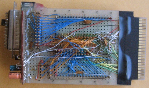
It shows up approximately actual size on my monitor. A card cage of those would be really compact and cute.
For things that need more connections, the 96-pin DIN 41612 connectors work nicely. They fit in standard hobbyist-friendly perfboard, and there are card cages available with these too. I have chosen this type of connector for my new workbench computer.
The rc2014 idea might work well, giving it a dual-row pin header of .025" square pins (like my memory module has) so a decent number of pins doesn't get so long. This configuration also allows boards that need some extra width.
Vector (and maybe other companies) used to supply 44-contact prototyping boards that plug into the Commodore 64, like this one I built some extra I/O onto:
It shows up approximately actual size on my monitor. A card cage of those would be really compact and cute.
For things that need more connections, the 96-pin DIN 41612 connectors work nicely. They fit in standard hobbyist-friendly perfboard, and there are card cages available with these too. I have chosen this type of connector for my new workbench computer.
http://WilsonMinesCo.com/ lots of 6502 resources
The "second front page" is http://wilsonminesco.com/links.html .
What's an additional VIA among friends, anyhow?
The "second front page" is http://wilsonminesco.com/links.html .
What's an additional VIA among friends, anyhow?
Re: Side Project - 65c02 ProtoBrick
GARTHWILSON wrote:
The main board should have all the basics on it, like some RAM, ROM, and I/O.
-
GARTHWILSON
- Forum Moderator
- Posts: 8773
- Joined: 30 Aug 2002
- Location: Southern California
- Contact:
Re: Side Project - 65c02 ProtoBrick
Tor wrote:
GARTHWILSON wrote:
The main board should have all the basics on it, like some RAM, ROM, and I/O.
http://WilsonMinesCo.com/ lots of 6502 resources
The "second front page" is http://wilsonminesco.com/links.html .
What's an additional VIA among friends, anyhow?
The "second front page" is http://wilsonminesco.com/links.html .
What's an additional VIA among friends, anyhow?
Re: Side Project - 65c02 ProtoBrick
I don't speak for everyone, but the reason having the CPU alone (for me) is that I want to build other systems that aren't based on the 6502.
The ColecoVision, for example, is a favorite of mine. A Z80 board and a 6502 board could use the same RAM/ROM boards. Especially if I keep their unique pins separate.
A ColecoVision clone is something I've always wanted to build. Especially since it's such a simple system.
The ColecoVision, for example, is a favorite of mine. A Z80 board and a 6502 board could use the same RAM/ROM boards. Especially if I keep their unique pins separate.
A ColecoVision clone is something I've always wanted to build. Especially since it's such a simple system.
Cat; the other white meat.

Re: Side Project - 65c02 ProtoBrick
It does seem to me that a modular system should separate RAM, ROM and I/O from the CPU, in order to allow experimentation with different memory maps (or even banking schemes.) It's not ideal for any specific setup, but the idea is to maximise flexibility.
-
BigDumbDinosaur
- Posts: 9425
- Joined: 28 May 2009
- Location: Midwestern USA (JB Pritzker’s dystopia)
- Contact:
Re: Side Project - 65c02 ProtoBrick
BigEd wrote:
It does seem to me that a modular system should separate RAM, ROM and I/O from the CPU, in order to allow experimentation with different memory maps (or even banking schemes.) It's not ideal for any specific setup, but the idea is to maximise flexibility.
x86? We ain't got no x86. We don't NEED no stinking x86!
-
GARTHWILSON
- Forum Moderator
- Posts: 8773
- Joined: 30 Aug 2002
- Location: Southern California
- Contact:
Re: Side Project - 65c02 ProtoBrick
BigEd wrote:
It does seem to me that a modular system should separate RAM, ROM and I/O from the CPU, in order to allow experimentation with different memory maps (or even banking schemes.) It's not ideal for any specific setup, but the idea is to maximise flexibility.
cbmeeks wrote:
I don't speak for everyone, but the reason having the CPU alone (for me) is that I want to build other systems that aren't based on the 6502.
The ColecoVision, for example, is a favorite of mine. A Z80 board and a 6502 board could use the same RAM/ROM boards. Especially if I keep their unique pins separate.
The ColecoVision, for example, is a favorite of mine. A Z80 board and a 6502 board could use the same RAM/ROM boards. Especially if I keep their unique pins separate.
http://WilsonMinesCo.com/ lots of 6502 resources
The "second front page" is http://wilsonminesco.com/links.html .
What's an additional VIA among friends, anyhow?
The "second front page" is http://wilsonminesco.com/links.html .
What's an additional VIA among friends, anyhow?
-
billylegota
- Posts: 60
- Joined: 31 Mar 2016
- Location: Austin, Texas
- Contact:
Re: Side Project - 65c02 ProtoBrick
I played around with such a design prior to designing my SBC. It certainly is not the most cost effective design, but it has the advantage of being fully modular.
Here are a few pics of my take on such a system.
CPU:
RAM / ROM:
Isometric Rendering:
Here are a few pics of my take on such a system.
CPU:
- Billy
-
billylegota
- Posts: 60
- Joined: 31 Mar 2016
- Location: Austin, Texas
- Contact:
Re: Side Project - 65c02 ProtoBrick
Continued due to max attachments...
The system has headers for the data, address, and other 6502 bus lines as well as connections to the rx and tx pins of the USB connector (could be used by a serial board).
- Billy
Re: Side Project - 65c02 ProtoBrick
Those are some nice designs.
Regarding the Z80/65c02 boards connecting to RAM/ROM...maybe I didn't explain very well. But the idea was to simply have all of the address and data lines in the same spot for CPU, RAM and ROM. A15-A0 is common. D7-D0 is common.
But yes, the I/O and "glue" logic would have to be jumpered or unique for Z80/65c02.
Cat; the other white meat.