Techniques for reliable high-speed digital circuits

Re: Techniques for reliable high-speed digital circuits
No, there are still parallel or lets say pseudo-parallel interfaces, there are also limitations for serial links. E.g. G.SHDSLbis bonding or LX4 or 1000BaseTX

Re: Techniques for reliable high-speed digital circuits
Here's a video on some aspects of high-speed digital circuits, specifically edge-rates, ringing, and termination, by Jack Ganssle, which kicks off by recommending a book, High Speed Digital Design by Johnson and Graham. Even secondhand, it's nearly £20, so it must be in demand.
I Only Probed the Board With a Scope - Why Did My Board Crash?
Also see Jack's newsletter "The Embedded Muse": archives at http://www.ganssle.com/tem-back.htm
(via this Hackaday post)
Edit: from the comments on that Hackaday post, see also the Tutorial section starting on page 15 of this application note: http://cds.linear.com/docs/en/applicati ... an47fa.pdf
Edit: also from the comments, a recommendation for the book "Right the first time" by Lee W. Ritchey, which is now a legitimate pdf download (signup required) at http://www.thehighspeeddesignbook.com/download.php
-
GARTHWILSON

- Forum Moderator
- Posts: 8773
- Joined: 30 Aug 2002
- Location: Southern California
- Contact:
Re: Techniques for reliable high-speed digital circuits
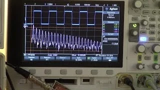
Thankyou Ed! That part from about 2:20 to 3:00, about the ugly ringing regardless of clock speed, so perfectly illustrates a point we've been trying to make for a long time. (I've seen worse, BTW.) I've kept many of Jack Ganssle's articles from magazines like Embedded Systems Programming from years ago, but I didn't realize he had youtube videos (I should have figured), and now I need to check out ganssle.com. (BTW, the reflections happen due to a mismatch of the load and the transmission line, not particularly the source. He alludes to that in the next video, regarding probes, starting at about 5:30. When I worked in VHF & UHF, I had to get pretty cozy with the Smith chart which is primarily about transmission lines.)
I've been hearing (reading about) Dr. Johnson's book for many years, and although I've never seen it, I get the idea that it's mostly the same material you can read in the articles at https://web.archive.org/web/20120302190 ... eyword.htm . There's a load of great reading there. [Edit: I did buy the book later.]
The LT applications notes .pdf file looks like it has loads of great stuff too. I'm going to dig in.
http://WilsonMinesCo.com/ lots of 6502 resources
The "second front page" is http://wilsonminesco.com/links.html .
What's an additional VIA among friends, anyhow?
The "second front page" is http://wilsonminesco.com/links.html .
What's an additional VIA among friends, anyhow?
Re: Techniques for reliable high-speed digital circuits
Nice index, thanks! I found this high-voltage visual demonstration of return current:
http://www.sigcon.com/Pubs/news/8_08.htm
http://www.sigcon.com/Pubs/news/8_08.htm
-
GARTHWILSON
- Forum Moderator
- Posts: 8773
- Joined: 30 Aug 2002
- Location: Southern California
- Contact:
Re: Techniques for reliable high-speed digital circuits
BigEd wrote:
Edit: from the comments on that Hackaday post, see also the Tutorial section starting on page 15 of this application note: http://cds.linear.com/docs/en/applicati ... an47fa.pdf
GARTHWILSON wrote:
The LT applications notes .pdf file looks like it has loads of great stuff too. I'm going to dig in.
I cannot believe this! Looking over this ap. note, it looks so good that I was thinking of getting the whole thing printed and putting it in a binder. I was writing an email to the other engineer in our company to recommend it, and I noticed the date, Aug '91; so I looked in my own books, and sure enough, in LT's 1993 Linear Applications Handbook Volume II, A Guide to Linear Circuit Design, there it was, along with a lot of other good ones, right next to Volume I which also has more. Don't throw away your old books. Dave Jones in one of his EEV blogs was saying it's stupid to keep them when everything is available online; but that's not always true. Another recent example that made me glad I kept the books is that TI has taken over NSC, but one of TI's shortcomings is that their data sheets don't have the helpful applications info that NSC's had, and where NSC's parts could cross-reference to TI's, they just replaced NSC's online data sheets with their own, causing us to lose that valuable info—except that in my case, I kept my three shelf-feet of NSC data books. I still wouldn't know (or remember) it was there though if you hadn't pointed it out, Ed.
http://WilsonMinesCo.com/ lots of 6502 resources
The "second front page" is http://wilsonminesco.com/links.html .
What's an additional VIA among friends, anyhow?
The "second front page" is http://wilsonminesco.com/links.html .
What's an additional VIA among friends, anyhow?
-
BigDumbDinosaur

- Posts: 9425
- Joined: 28 May 2009
- Location: Midwestern USA (JB Pritzker’s dystopia)
- Contact:
Re: Techniques for reliable high-speed digital circuits
BigEd wrote:
Nice index, thanks! I found this high-voltage visual demonstration of return current:
http://www.sigcon.com/Pubs/news/8_08.htm
http://www.sigcon.com/Pubs/news/8_08.htm
Joking aside, thanks for posting the link. Very interesting.
x86? We ain't got no x86. We don't NEED no stinking x86!

Re:
GARTHWILSON wrote:
Ok, I took a picture of one of mine, a 44-pin, from Aries (although they no longer supply it):
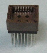
It's no bigger than a standard thru-hole one.
[Edit, 1/21/13: BigEd just pointed us to a source that stocks them: http://uk.rs-online.com/web/c/?searchTe ... ra=oss&r=t ]
It's no bigger than a standard thru-hole one.
[Edit, 1/21/13: BigEd just pointed us to a source that stocks them: http://uk.rs-online.com/web/c/?searchTe ... ra=oss&r=t ]
Be sure to use proto-board whose holes are plated through, as they offer better solder adhesion and thus more mechanical support. You don't want any pins twisting off during the wrap process. That could be tricky to fix if the neighboring pins are already wrapped and the region is congested with wire.
If your luck is bad, such a particle could lodge itself invisibly underneath the PLCC socket or some other component, and it would be impossible to detect and fix. I'm not a worrier by nature but I am uncomfortable with a power plane on the top (component side). The board in the photos is from Twin Industries, and they offer a double-sided power plane version as well. But I'll settle for a ground plane on the wiring side (bottom) only, where gravity isn't attracting debris, and where you have a better chance of seeing & correcting any trouble.
cheers,
Jeff
In 1988 my 65C02 got six new registers and 44 new full-speed instructions!
https://laughtonelectronics.com/Arcana/ ... mmary.html
https://laughtonelectronics.com/Arcana/ ... mmary.html
-
GARTHWILSON
- Forum Moderator
- Posts: 8773
- Joined: 30 Aug 2002
- Location: Southern California
- Contact:
Re: Techniques for reliable high-speed digital circuits
I like plan B, because it makes for shorter connections (and therefore less inductance) from the planes to the IC.
When there's a possibility that's anything like that, you measure as you put each part on (in this case, the socket or a pin), so that if a problem shows up, you know it's at the part you did last. If you wait until you're done and admiring your handiwork to check and find a problem, you won't know where it is. I have to do this with the embedded bypass capacitors I put in my memory modules. Those embedded capacitors resulted in more manual labor than I bargained for, but I think they're still worth it (marginally).
Whether you use a single plane or double, solder a chip capacitor from each Vcc pin to the ground plane around it. It will have absolutely no lead length. That's the way we want it for best high-frequency behavior.
Quote:
If your luck is bad, such a particle could lodge itself invisibly underneath the PLCC socket or some other component, and it would be impossible to detect
When there's a possibility that's anything like that, you measure as you put each part on (in this case, the socket or a pin), so that if a problem shows up, you know it's at the part you did last. If you wait until you're done and admiring your handiwork to check and find a problem, you won't know where it is. I have to do this with the embedded bypass capacitors I put in my memory modules. Those embedded capacitors resulted in more manual labor than I bargained for, but I think they're still worth it (marginally).
Whether you use a single plane or double, solder a chip capacitor from each Vcc pin to the ground plane around it. It will have absolutely no lead length. That's the way we want it for best high-frequency behavior.
http://WilsonMinesCo.com/ lots of 6502 resources
The "second front page" is http://wilsonminesco.com/links.html .
What's an additional VIA among friends, anyhow?
The "second front page" is http://wilsonminesco.com/links.html .
What's an additional VIA among friends, anyhow?
Re: Techniques for reliable high-speed digital circuits
GARTHWILSON wrote:
I like plan B, because it makes for shorter connections (and therefore less inductance) from the planes to the IC.
Quote:
solder a chip capacitor from each Vcc pin to the ground plane around it
In 1988 my 65C02 got six new registers and 44 new full-speed instructions!
https://laughtonelectronics.com/Arcana/ ... mmary.html
https://laughtonelectronics.com/Arcana/ ... mmary.html
-
BigDumbDinosaur
- Posts: 9425
- Joined: 28 May 2009
- Location: Midwestern USA (JB Pritzker’s dystopia)
- Contact:
Techniques for reliable high-speed digital circuits
Attached is a white paper by Cypress Semiconductor that discusses various aspects of good system board design, especially as related to bypassing components and the effects of internal ground and power layers. Although Cypress' main product is static RAM of various types, the paper is applicable to all aspects of digital design.
- Attachments
-
- SRAM_board_design_guidelines.pdf
- SRAM System Board Design White Paper
- (822.24 KiB) Downloaded 807 times
x86? We ain't got no x86. We don't NEED no stinking x86!
-
Oneironaut

- Posts: 734
- Joined: 25 May 2015
- Location: Gillies, Ontario, Canada
- Contact:
Re: Techniques for reliable high-speed digital circuits
Although my take on getting speed out of a digital circuit has more to do with design than hardware, it may be of some use!
In several recent projects that generate VGA from logic components, propagation delay became the limiting factor. Using 10ns SRAM and all 74HC logic, my propagation delays ranged from 10ns (74HC245 Buffer) to just under 20ns (74HC574 setup time).
So with a clock speed of 25.175MHz for standard 640x480 VGA, this mean that on every single clock cycle, the complete path from counter to output could not exceed 39 nanoseconds. Now this is a far stretch for a circuit built out of noting but 7400 logic chips that needs to address half a meg of SRAM, keep track of the address, send it through a switch, and then output it to an R2R DAC with all sync signals included!
When I lay out a design like this, I think in terms of propagation delay and then choose the appropriate IC for the job. Knowing that 3 chained 74HC193 counters will require about 20ns of time, this leaves only 19ns of time (39-20). Now subtract the 10ns output time for the SRAM and I am left with only 9ns, which is not enough time for the signal to propagate through the next 2 buffers (74HC574).
So now what?... give up and do another FPGA design? Get a Raspberry PI? .... no way, just throw more silicon at it!
My magic trick is to add a register to the signal path everytime I exceed the maximum allowed propagation delay.
I like to use the 74HC574 (8-bit positive-edge triggered D-type flip-flop) to hold back my data one clock cycle.
So now the 574 captures the signal at the 19ns mark, which is just within its 18ns required setup time.
On the next clock cycle, the 574 releases its data at a rate of 16ns, so now I can continue my propagation count.
With 2 more buffers ahead of the signal, each requiring 16ns, I still can't send the signal all the way to the DAC.
No problem, just toss in another 574 to capture the signal and then send it out on the third clock cycle.
By adding 2 more register levels, I am now able to keep the worst case scenario to 34ns, which is under the 39ns maximum.
This system has worked well for many of my designs, which often push up to 40MHz on a breadboard.
In my FPGA designs, adding "another register level" can also be a cure for accessing external devices that can't keep up.
So that's my 2 nanoseconds worth of advice for the High Speed Thread!
If you can't get the signal there in time, give it a break until the next clock pulse.
And as for bread-boaring High Speed Logic... don't let anyone tell you that 40MHz is impossible!
Cheer,
Radical Brad
Re: Techniques for reliable high-speed digital circuits
What about exotic physics-based ideas? Would cooling such a device to below-zero temps, using ecl, asynchronous logic, or 3d printing a cpu so components can be placed directly above/below each other and therefore get much closer to each other increase speed significantly?
Re: Techniques for reliable high-speed digital circuits
Certainly you can get more speed if you apply cooling. Indeed, you don't even need the cooling - if you know your chip temperatures won't go too high then they will run faster than worst-case, and the specs are always worst-case.
Last edited by BigEd on Sun Jun 12, 2016 7:13 pm, edited 2 times in total.
-
GARTHWILSON
- Forum Moderator
- Posts: 8773
- Joined: 30 Aug 2002
- Location: Southern California
- Contact:
Re: Techniques for reliable high-speed digital circuits
nonanon wrote:
What about exotic physics-based ideas? Would cooling such a device to below-zero temps, using ecl, asynchronous logic, or 3d printing a cpu so components can be placed directly above/below each other and therefore get much closer to each other increase speed significantly?
Temperature definitely has an effect (hotter=slower) but not as major as you might think. With Peltier devices being easily available, I thought about using one several years ago, but was disappointed to find out from the data sheets that while the speed difference may be somewhat significant for some applications, it is not huge.
Samuel Falvo (kc5tja here on the forum) posted years ago about making the processor asynchronous. I'll edit this and put in a link if/when I find it. At the speeds our stuff works at, distance is not a problem if the board is, say, 100x160mm (3U Eurocard sized). Depending on the layout though, it may reduce capacitance on the lines and reduce problems from transmission-line effects not being handled right. Ed had a recent post on stacking ICs in the topic "OT: stacked (DIP) chips."
http://WilsonMinesCo.com/ lots of 6502 resources
The "second front page" is http://wilsonminesco.com/links.html .
What's an additional VIA among friends, anyhow?
The "second front page" is http://wilsonminesco.com/links.html .
What's an additional VIA among friends, anyhow?
-
GARTHWILSON
- Forum Moderator
- Posts: 8773
- Joined: 30 Aug 2002
- Location: Southern California
- Contact:
Re: Techniques for reliable high-speed digital circuits
GARTHWILSON wrote:
Samuel Falvo (kc5tja here on the forum) posted years ago about making the processor asynchronous. I'll edit this and put in a link if/when I find it.
I remembered the search terms to find it. It's in this topic: "idea: a cell-like chip based on many 6502 cores," in the context of multiprocessing.
http://WilsonMinesCo.com/ lots of 6502 resources
The "second front page" is http://wilsonminesco.com/links.html .
What's an additional VIA among friends, anyhow?
The "second front page" is http://wilsonminesco.com/links.html .
What's an additional VIA among friends, anyhow?