In order to interface to a development board, I need to be able to route the 816 bus off the board unfortunately.
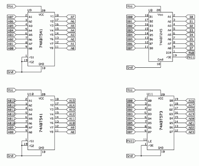
In which case, I suggest you look at using drivers for the address bus (74AC541, for example, two required) and a transceiver (74AC245) for the data bus. The drivers and transceiver will help to mitigate the effects of bus loading. Note that everything should be on the "downstream" side of the drivers and transceiver to avoid inadvertent signal skew. Bus termination will likely be necessary to control ringing, an area where you may have to experiment to achieve satisfactory results. Thevenin termination may suffice if the aggregate bus length isn't too great.
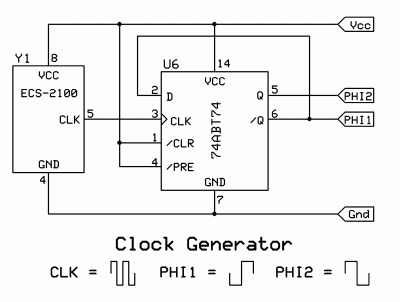
You will also need a latch for capturing the bank address (74ABT573 or 74AC573, the former is the faster part) and a two-phase clock generator to control the latch and transceiver output-enables. See attached clock generator schematic, as well as bus logic example—
ABx and
DBx connections on the drivers, latch and transceiver are connected to the MPU's address and data bus pins, respectively.
Note that use of the clock to determine when the transceiver should be active doesn't automatically meet the requirement of not reading or writing during Ø2 low. That is accomplished by qualifying
RWB with Ø2. Such qualification is not necessary with the W65C21x, W65C22x and W65C51x, and
should not be applied—connect
RWB of these devices directly to
RWB on the 65C816.
Also note that
VDA and
VPA must be consulted in determining when to latch the bank address. A number of instructions cause the '816 to generate false address bus states during intermediate execution steps, especially when indexing is involved to determine the effective address. If the expression
VDA | VPA is false (
| meaning logical OR) then the address bus content is undefined and chip enables must not be asserted. However, during that time, your DMA controller could temporarily become the bus master by negating
BE—the '816 will continue with what it is doing. If one or two "dead" cycles don't give the controller enough time to accomplish anything, then it will have to "forceably" kick the MPU off the buses by negating
RDY and
BE (in that order), do its work and then restart the MPU by releasing
BE and
RDY (in that order). The
MLB signal would have to be factored into any bus mastering as well.
If I design a preliminary bus "standard", would someone be willing to critique it for me? My dev board uses a 40-pin male IDE connector for GPIO, so I'd need to use a female IDE connector that solders underneath the PCB. I know this is explicitly not recommended in the primer- I'm willing to take the risks to life, property, and my assets in this case.
As long as you understand the perils and promise not to sue us, we'll try to help out.

Jocosity aside, a viable expansion bus design, that is, one into which cards could be plugged, is better developed so that it is isolated from the MPU bus, a la PCI in modern x86 machines. This could be accomplished with the W65C21 or W65C22, or similar devices. Use of peripheral silicon to drive the expansion bus instead of attaching it to the MPU's buses means that the expansion bus becomes a memory-mapped "I/O device," and thus can't affect the MPU unless the latter allows it to. It also means that the expansion bus speed can be independent of the Ø2 clock rate. There is a bit more to this than just wiring some address and data lines to some connectors.
I'm actually doing the paper design now... I'll start out simple, as suggested in previous posts... '816, RAM, ROM, VIA, 6551, and two banks (mix of code/data, or one code and one data- haven't decided yet).
It would probably be wise to not segregate code and data. If you are thinking about implementing a Harvard architecture, you can only do part of it. A true Harvard machine has the code and data storage physically separated and connected to the MPU by different buses. You wouldn't be able to have separate buses with the '816. Just an opinion, but I see no upside to trying to go the Harvard route in a hobby machine.
You always have the option to load your program wherever you choose, as long as it is no longer than 64K. Data can exceed 64K, as indexing past the end of one bank always temporarily increments to the next bank (but doesn't actually change
DB). You can also use indirect indexed long addressing (e.g.,
LDA [$80],Y) to reach out to any bank and span into the next one.
And besides, might as well USE the not widely used features of the '816

.
I've been an advocate of that all along.

You'll get ample opportunity when you reach the stage of trying to implement DMA.

- Two-Phase Clock Generator

- 65C816 Bus Drivers & Bank Latch Example