6502 Design & concept questions.

For discussing the 65xx hardware itself or electronics projects.
User avatar
Arlet
Posts: 2353
Joined: 16 Nov 2010
Location: Gouda, The Netherlands
Contact:

Re: 6502 Design & concept questions.

Post by Arlet »

lordbubsy wrote:
That’s not bad, for a more permanent supply I would use this schematic from a commercial product.
I would move C4 to the other side of the diode, so it's connected to the 7806. That is, if you insist on 7806+diode. I'd rather replace it by a 5V regulator without the diode. The diode isn't really doing anything useful.
lordbubsy
Posts: 207
Joined: 11 Sep 2013
Location: The Netherlands

Re: 6502 Design & concept questions.

Post by lordbubsy »

Arlet wrote:
The FPGA will then become a super peripheral, capable of supporting video, sound, SPI, GPIO, USB, timers, UART, Flash, and whatever else I'd like. Using the BE pin, the FPGA can take over the bus, and pre-init SRAM, perform DMA, and generate video.
That sounds really great, I can’t wait to see it happen and perhaps learn something from it.
Quote:
if you insist on 7806+diode.
you’re right, it doesn’t make much sense in this case.
But further you have some flexibility on providing your circuit with power.
Marco
User avatar
GARTHWILSON
Forum Moderator
Posts: 8773
Joined: 30 Aug 2002
Location: Southern California
Contact:

Re: 6502 Design & concept questions.

Post by GARTHWILSON »

Arlet wrote:
I would move C4 to the other side of the diode, so it's connected to the 7806. That is, if you insist on 7806+diode. I'd rather replace it by a 5V regulator without the diode. The diode isn't really doing anything useful.
Yes, put the bigger capacitor on the input of the regulator, not the output. Also, use a 5V regulator with no diode in the output (the diode makes for much poorer regulation), but:
Quote:
But further you have some flexibility on providing your circuit with power.
If you want to power it other ways to, put that diode across the regulator, with its anode at the output and its cathode at the input, then you can power the circuit from other sources if you like, without disconnecting the regulator and without hurting anything.
http://WilsonMinesCo.com/ lots of 6502 resources
The "second front page" is http://wilsonminesco.com/links.html .
What's an additional VIA among friends, anyhow?
User avatar
GARTHWILSON
Forum Moderator
Posts: 8773
Joined: 30 Aug 2002
Location: Southern California
Contact:

Re: 6502 Design & concept questions.

Post by GARTHWILSON »

Arlet wrote:
I also recommend making a ground plane on top and bottom, and start by trying to route your signals on bottom layer. Many folks advocate using a power plane, but for 2 layer boards, I recommend sticking with 2 ground planes, and some fat power traces
and, I would add, put the bypass capacitors as close to the Vcc pins as you can.
Quote:
The reason is that your signals are going to chop up your ground plane, and if you only have one, you'll end up with a bunch of broken pieces. If you have two ground planes, and a bunch of vias connecting them, they'll work together as one solid plane.

(emphasis added). So where you have traces crossing on opposite layers, getting best AC behavior will involve putting four vias in the ground planes as close as practical to each of the four corners where the traces cross, so the ground return path for any given signal can stay as close as possible to the signal line. More on good construction and layout are in our sticky topic "Techniques for reliable high-speed digital circuits and the links there.

Again though, at 1 or 2MHz, you can get away with murder. [Edit: I must clarify that that refers to timings. If you have fast parts, you still have to keep your nose clean regarding build technique, as poor build technique can bite you even at very low clock rates.]
http://WilsonMinesCo.com/ lots of 6502 resources
The "second front page" is http://wilsonminesco.com/links.html .
What's an additional VIA among friends, anyhow?
User avatar
Arlet
Posts: 2353
Joined: 16 Nov 2010
Location: Gouda, The Netherlands
Contact:

Re: 6502 Design & concept questions.

Post by Arlet »

GARTHWILSON wrote:
If you want to power it other ways to, put that diode across the regulator, with its cathode at the output and its anode at the input, then you can power the circuit from other sources if you like, without disconnecting the regulator and without hurting anything.
I don't think that's going to work if you offer, say, 12V at the input.

I think the idea of the diode after the regulator is that you can add another power source, also with its own diode, and attach it to the same point.

Another note about the schematic: I like to have the current flow from left to right (unless it's a feedback), so I'd flip the whole thing. Similarly, I always put my VCC at the top, and GND at the bottom, and also keep the VCC/GND symbols always facing the proper way. It just bugs me to see a GND symbol turned upside down, just because there was no room in the schematic.
User avatar
GARTHWILSON
Forum Moderator
Posts: 8773
Joined: 30 Aug 2002
Location: Southern California
Contact:

Re: 6502 Design & concept questions.

Post by GARTHWILSON »

Arlet wrote:
GARTHWILSON wrote:
If you want to power it other ways to, put that diode across the regulator, with its cathode at the output and its anode at the input, then you can power the circuit from other sources if you like, without disconnecting the regulator and without hurting anything.
I don't think that's going to work if you offer, say, 12V at the input.
Woops, you're right-- I got it backwards. I'll edit it. I don't want to steer anyone wrong. I guess having the circuit drawn right-to-left turned my thinking backwards. I just need to slow down.
http://WilsonMinesCo.com/ lots of 6502 resources
The "second front page" is http://wilsonminesco.com/links.html .
What's an additional VIA among friends, anyhow?
User avatar
Arlet
Posts: 2353
Joined: 16 Nov 2010
Location: Gouda, The Netherlands
Contact:

Re: 6502 Design & concept questions.

Post by Arlet »

GARTHWILSON wrote:
Again though, at 1 or 2MHz, you can get away with murder.
Agreed, but I always like to make the designs as robust as possible. Paying a little extra care to layout doesn't cost anything (except a bit of time).

Also, having a nice ground plane also improves immunity against external electromagnetic fields.
User avatar
Arlet
Posts: 2353
Joined: 16 Nov 2010
Location: Gouda, The Netherlands
Contact:

Re: 6502 Design & concept questions.

Post by Arlet »

GARTHWILSON wrote:
I guess having the circuit drawn right-to-left turned my thinking backwards. I just need to slow down.
That's why I'd take the time to flip it over. Consistency helps prevent silly mistakes.
User avatar
GARTHWILSON
Forum Moderator
Posts: 8773
Joined: 30 Aug 2002
Location: Southern California
Contact:

Re: 6502 Design & concept questions.

Post by GARTHWILSON »

Arlet wrote:
GARTHWILSON wrote:
Again though, at 1 or 2MHz, you can get away with murder.
Agreed, but I always like to make the designs as robust as possible. Paying a little extra care to layout doesn't cost anything (except a bit of time).
Agreed, and I would always do it the best I can too—I just don't want to scare newcomers off with too much theory if they're using 1MHz parts and it won't be necessary for just making it work.

Quote:
Also, having a nice ground plane also improves immunity against external electromagnetic fields.

and even more importantly, against radiating electrical noise that can get into sensitive nearby analog circuits, especially ones that might be controlled by this computer.
http://WilsonMinesCo.com/ lots of 6502 resources
The "second front page" is http://wilsonminesco.com/links.html .
What's an additional VIA among friends, anyhow?
lordbubsy
Posts: 207
Joined: 11 Sep 2013
Location: The Netherlands

Re: 6502 Design & concept questions.

Post by lordbubsy »

This is a link to the crime scene.
http://shop.myavr.com/Kits/myAVR%20Boar ... p&artID=41

On the right you can check the circuit diagram.

It seems they have that circuit as a separate product.
http://shop.myavr.com/Kits/externPowerK ... tID=100003
Arlet wrote:
I think the idea of the diode after the regulator is that you can add another power source,
you’re right, the programmer on that board can also supply the voltage.
Arlet wrote:
I just don't want to scare newcomers off with too much theory if they're using 1MHz parts and it won't be necessary for just making it work.
Well, a lot of things that were explained I understand, but some I don’t. But I think it’s useful to get all that information. At a later time when I read it elsewhere I might get some recognition and perhaps understand it (better).

Till now I have switched course quite a few times while implementing new insights, which in itself is rather frustrating. But it saved me some unnecessary work already.
Marco
lordbubsy
Posts: 207
Joined: 11 Sep 2013
Location: The Netherlands

Re: 6502 Design & concept questions.

Post by lordbubsy »

Reporting some progress:
I finished making a Xilinx parallel programmer and a XC9536 / 72 ISP Demo Board.
I also managed to reproduce Daryl’s 65SPI. I’m really happy. 8-P

Daryl is helping me programming some address decoding (thanks Daryl) and it’s going well. I’m studying an HDL-ABEL Primer and found Xilinx’s ABEL Reference Guide
http://www.xilinx.com/itp/xilinx10/help ... /whnjs.htm

I’ve attached the demo board to my prototype 6502 and transferred my very first bytes through 65SPI. As slave device I connected a gameduino. (not on the picture)
005.jpg
2.png
Marco
User avatar
barrym95838
Posts: 2056
Joined: 30 Jun 2013
Location: Sacramento, CA, USA

Re: 6502 Design & concept questions.

Post by barrym95838 »

Please forgive me if the answer is obvious, but what is that sub-microsecond spike in the green channel?

Mike
lordbubsy
Posts: 207
Joined: 11 Sep 2013
Location: The Netherlands

Re: 6502 Design & concept questions.

Post by lordbubsy »

I suspect that it is the start of the third byte, which has to be “1” on start. I’m not sure though.

OTH, I discovered that transmission wasn’t stable. Therefore I have replaced the power form the USB cable to a proper power supply. I lowered PHI2 to 1MHz instead of 1.8432MHz. Cleaned up the breadboard and added some more bypass caps. That didn’t help either.
After I connected ALL VCC’s, GND’s and open inputs to GND from 65SPI, transmission stays stable.
CRW_0009.jpg
Although I keep getting random spikes on all channels.

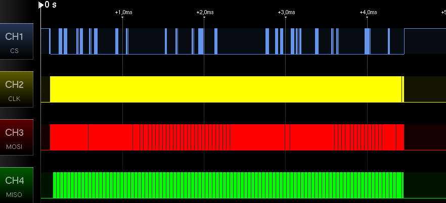
This is the start of the transmission which sends $80, $00, "abcdefgh etc."
Clipboard01.png
This is the whole transmission.
Clipboard02.png
Clipboard02.png (7.02 KiB) Viewed 982 times
All those blue spikes shouldn't be there.
I hope it will be more stable on the PCB. I’m at roughly 80% now.
Marco
Post Reply