The timing of your post is amazing. I have to seriously start considering purchasing the tools very soon. My project cannot fit the pseudo random number generator and the timer with everything else and maintain 100MHz with the 144-pin Spartan 6. Up to 14 modules now, and I still have more to do with the video mixing.
With a package using more pins I could do what I wanted to do and utilize the 2 parity bits on the address lines of the SyncRAM and assign 4 math/logic functions to every pixel.
I will start searching out a good size Spartan 6. Thanks for the inspiration!
EDIT: Added detail. Was busy day at work when I had posted earlier.
Working with Xilinx BGA packages
-
ElEctric_EyE
- Posts: 3260
- Joined: 02 Mar 2009
- Location: OH, USA

Re: Working with Xilinx BGA packages
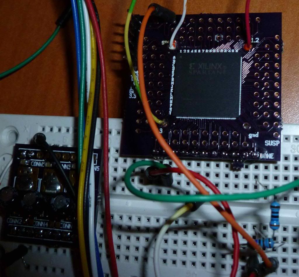
XC3S200AN 256-pin BGA successfully mounted. It configures, and I've tested a bunch of the connected pins with an LED blinker circuit...
Soldered using a hunk-of-aluminum PID hotplate, homemade.
I am sick of the flaky breadboards, though. Anyone else interested in a wire-wrap breakout board for BGA chips?
Soldered using a hunk-of-aluminum PID hotplate, homemade.
I am sick of the flaky breadboards, though. Anyone else interested in a wire-wrap breakout board for BGA chips?
In theory, there is no difference between theory and practice. In practice, there is. ...Jan van de Snepscheut
Re: Working with Xilinx BGA packages
I would like to report another mounting success, this time with a 484 BGA package:
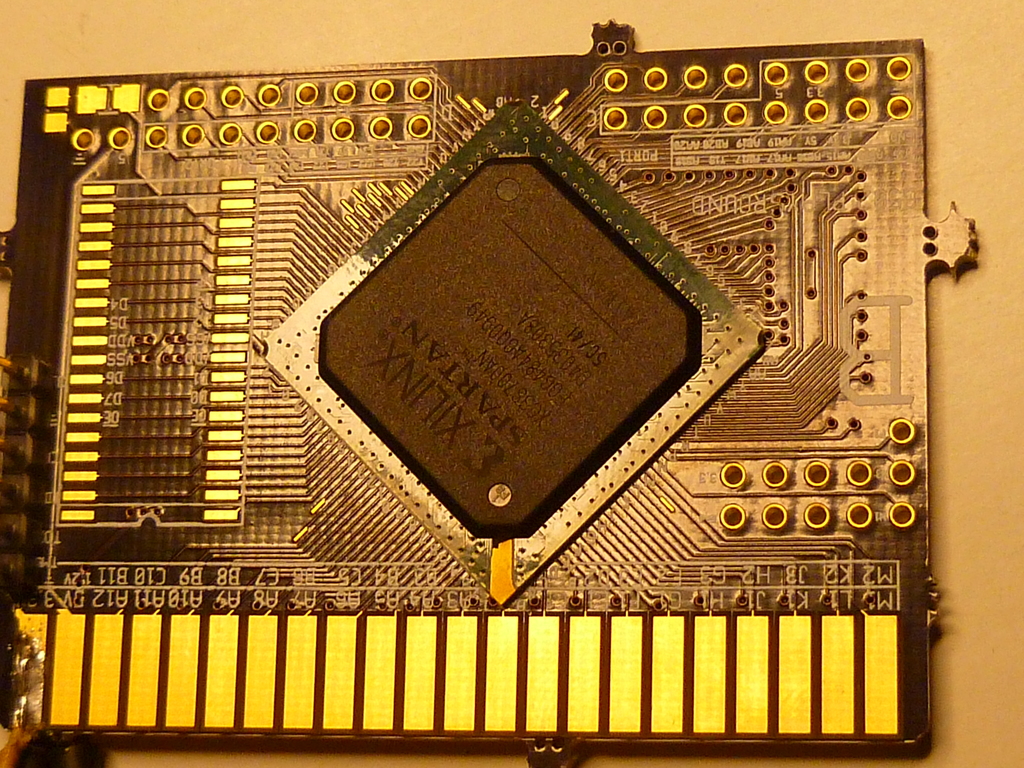
Here is an edge view, showing how you can see underneath the chip. This gives you a pretty good indication that there are no shorts - you can see down the entire grid!
I soldered down 3 of these BGAs perfectly.
Unfortunately my PCB had an error with power distribution, so the board is running hot because the VCCINT bus is being fed 3.3V. Amazingly it works (who knows for how long though) - see viewtopic.php?f=10&t=2328&start=15
Here is an edge view, showing how you can see underneath the chip. This gives you a pretty good indication that there are no shorts - you can see down the entire grid!
Unfortunately my PCB had an error with power distribution, so the board is running hot because the VCCINT bus is being fed 3.3V. Amazingly it works (who knows for how long though) - see viewtopic.php?f=10&t=2328&start=15
Last edited by enso on Tue Jun 11, 2013 1:51 am, edited 1 time in total.
In theory, there is no difference between theory and practice. In practice, there is. ...Jan van de Snepscheut
-
ElEctric_EyE
- Posts: 3260
- Joined: 02 Mar 2009
- Location: OH, USA
Re: Working with Xilinx BGA packages
Very good news! Nice to hear you figured out your issue with VCCint and VCCaux... So you have a 2 layer board and a 484-pin device. How many of the pins are unused? I am itching to start a new design and tackle a larger Spartan 6. Thanks for posting.
Re: Working with Xilinx BGA packages
BGA484 is greatly underutilized in my case, but it was more than enough IOs for my purposes.
With a two-layer board, in the ideal case you can bring out 4 rows (2 on top layer and 2 on the bottom layer), from each of the 4 sides. In practice (once you try you'll see why) the yield is lower. But with 22 rows of pins, even 2 layers gives you 22 x 4 = 88 pins, and you can easily take out more than 100.
If you need a lot more, I would just use the BGA 1154 package, with rows of 34 pins. You can easily take 400 pins out of that one, and the wider chip gives you more room to route around - not to mention that there are more goodies inside!
My thinking is to not worry too much about the 'wasted' pins, and just enjoy myself...
I do want to point out that if you plan to make a fast core using Spartan6, consider that not having a groundplane may be problematic...
Here is the relevant piece of the PCB: (Click to enlarge. .) Note there are a few IO lines that I just didn't have room to route anywhere, so I attached them to long narrow pads that can be used to attach wire-wrap wire for future expansion.
- Attachments
-
Last edited by enso on Tue Jun 11, 2013 1:56 am, edited 1 time in total.
In theory, there is no difference between theory and practice. In practice, there is. ...Jan van de Snepscheut
-
ElEctric_EyE
- Posts: 3260
- Joined: 02 Mar 2009
- Location: OH, USA
Re: Working with Xilinx BGA packages
How much cost and what parts were involved in your PID hotplate custom construction? I think you laid out a few parts for your thread in the hardware section? or somewhere, but not really any of the full details. If I missed the thread just point there. I remember an aluminum block with 2 connections.
Re: Working with Xilinx BGA packages
Parts for the hotplate:
Make sure the PID controller can use a thermocouple - I think all of them can.
Heaters and thermocouples come in all sizes - pick one that will fit inside your aluminum block.
Once you have them, drill your block. Don't even think about using a hand drill, use a good, long-travel drill press or you'll be sorry. I was sorry - my drill press could not travel far enough, and my drill bit was too short. Needless to say, using the wrong tools just makes your job harder - each hole required readjustments of the drill press mid-drilling.
Then insert heating elements and the 'couple. Mine was big enough for 2 heaters - a single one for a smaller block is probably fine. The thermocouple hole was threaded, the heaters just pressure-fit into holes.
The rest is making electrical connections and deciphering the PID instructions. I used the default PID tuning settings - it's good enough. Pulses the heaters about once per second.
I am not sure if the hotplate is really better than an oven. For experimenting, definitely - you can see your board better. But an oven is better for attaching lots of chips on both sides of the board.
- aluminum block. Size not too important; mine is about 1" x 4" x 7"
pid controller
ssr - solid state relay
thermocouple
heating elements - I used 2 x 500W units (it takes about 10min to heat up to 250C)
Make sure the PID controller can use a thermocouple - I think all of them can.
Heaters and thermocouples come in all sizes - pick one that will fit inside your aluminum block.
Once you have them, drill your block. Don't even think about using a hand drill, use a good, long-travel drill press or you'll be sorry. I was sorry - my drill press could not travel far enough, and my drill bit was too short. Needless to say, using the wrong tools just makes your job harder - each hole required readjustments of the drill press mid-drilling.
Then insert heating elements and the 'couple. Mine was big enough for 2 heaters - a single one for a smaller block is probably fine. The thermocouple hole was threaded, the heaters just pressure-fit into holes.
The rest is making electrical connections and deciphering the PID instructions. I used the default PID tuning settings - it's good enough. Pulses the heaters about once per second.
In theory, there is no difference between theory and practice. In practice, there is. ...Jan van de Snepscheut
Re: Working with Xilinx BGA packages
Some thoughts on mounting BGAs at home
After much trial and error, I would like to tell you this:
BGAs are well within the realm of an advanced hobbyist! In fact, BGAs are easier than TQFPs
After much trial and error, I would like to tell you this:
BGAs are well within the realm of an advanced hobbyist! In fact, BGAs are easier than TQFPs
- 1mm is easier to place than 0.5mm.
Don't use solderpaste (m̶y̶ ̶P̶C̶B̶ ̶v̶e̶n̶d̶o̶r̶ ̶g̶o̶l̶d̶-̶p̶l̶a̶t̶e̶s̶ ̶t̶h̶e̶ ̶b̶o̶a̶r̶d̶s̶,̶ ̶o̶t̶h̶e̶r̶ ̶f̶i̶n̶i̶s̶h̶e̶s̶ ̶m̶a̶y̶ ̶r̶e̶q̶u̶i̶r̶e̶ ̶p̶a̶s̶t̶e̶). [2021 edit: No gold-plated boards! Use regular tinned boards and no paste! ] Just liquid flux from a pen. Balls melt enough to provide a solid connection. Without paste, you can move the chip around until it pops into the dips made by the soldermask, so placing is easy! You hardly need a magnifier.
Hotplate makes the process easy as you can see the balls soften and the chip slump. You can then gently remove your board and cool it. I ruined a number of BGAs in the oven by over and undercooking. My oven is not PID controlled. If you are more scientific about it, you will be able to do it, but with a plate you can just watch the balls.
Prepare to ruin a few chips before getting the hang of it. I ruined a few because of solderpaste, which is a bad idea. As it melts, it transfers too much heat to the balls, and the whole chip just crashes down squeezing molten solder out the side.
You don't need an X-ray machine! You can look at your BGA from the side, right through every row of balls to verify that there are no shorts. And the balls themselves around the edges give you a very good idea of how well the part is attached. If it's symmetrical and the edge balls are well-formed, and you can see through it, you are done. I haven't had a single problem yet.
The hard part is not the soldering, it's laying out an error-free circuit connecting all those pads under the chip. Breaking out from the grid is a real puzzle - you can't put vias under pins (they suck solder right out); there is only one place to put a via - smack in between 4 pads. Once you put a via, you can't put a wire there, so it's a lot like a Rubik's cube.
All PCB layout packages simply stink when it comes to dense BGA grids. I use gEDA PCB - it's quirky but at least it's opensource and the files are text-based, so I can generate tricky footprints or adjust placement of things with a text editor on occasion.
Last edited by enso on Tue Jun 29, 2021 2:14 am, edited 1 time in total.
In theory, there is no difference between theory and practice. In practice, there is. ...Jan van de Snepscheut
-
GARTHWILSON

- Forum Moderator
- Posts: 8775
- Joined: 30 Aug 2002
- Location: Southern California
- Contact:
Re: Working with Xilinx BGA packages
enso wrote:
you can move the chip around until it pops into the dips made by the soldermask, so placing is easy! You hardly need a magnifier.
Quote:
My oven is not PID controlled. If you are more scientific about it, you will be able to do it, but with a plate you can just watch the balls.
Quote:
The hard part is not the soldering, it's laying out an error-free circuit connecting all those pads under the chip. Breaking out from the grid is a real puzzle - you can't put vias under pins (they suck solder right out)
Quote:
All PCB layout packages simply stink when it comes to dense BGA grids. I use gEDA PCB - it's quirky but at least it's opensource and the files are text-based, so I can generate tricky footprints or adjust placement of things with a text editor on occasion.
http://WilsonMinesCo.com/ lots of 6502 resources
The "second front page" is http://wilsonminesco.com/links.html .
What's an additional VIA among friends, anyhow?
The "second front page" is http://wilsonminesco.com/links.html .
What's an additional VIA among friends, anyhow?

Re: Working with Xilinx BGA packages
GARTHWILSON wrote:
Should I assume that the BGA manufacturers have pad-size recommendations like manufacturers have for other packages? Should the holes in the soldermask be only big enough to ensure that there's no gasketing (which would mean only about .002" or .004" greater diameter than the pad if it's LPI)?
Re: Working with Xilinx BGA packages
enso wrote:
Don't use solderpaste (my PCB vendor gold-plates the boards, other finishes may require paste). Just liquid flux from a pen. Balls melt enough to provide a solid connection. Without paste, you can move the chip around until it pops into the dips made by the soldermask, so placing is easy! You hardly need a magnifier.
-
GARTHWILSON
- Forum Moderator
- Posts: 8775
- Joined: 30 Aug 2002
- Location: Southern California
- Contact:
Re: Working with Xilinx BGA packages
Arlet wrote:
Yes, the BGA manufacturers generally have good recommendations with respect to pads, soldermask, clearance, traces and vias. See for instance Xilinx Device Package User Guide.
http://WilsonMinesCo.com/ lots of 6502 resources
The "second front page" is http://wilsonminesco.com/links.html .
What's an additional VIA among friends, anyhow?
The "second front page" is http://wilsonminesco.com/links.html .
What's an additional VIA among friends, anyhow?
Re: Working with Xilinx BGA packages
GARTHWILSON wrote:
What kind of soldermask? Would this work with LPI, or only with wet-screened? (Is LPI thick enough to do this?)
Quote:
Would an electric skillet work?
Quote:
What if you fill the via with solder first? It kind of sounds like the BGA manufacturers almost assume you're going to make a multilayer board with blind and burried vias. That's not cheap stuff.
Quote:
I use an old DOS version of Easy-PC Pro....
Thanks for your input
In theory, there is no difference between theory and practice. In practice, there is. ...Jan van de Snepscheut
-
ElEctric_EyE
- Posts: 3260
- Joined: 02 Mar 2009
- Location: OH, USA
Re: Working with Xilinx BGA packages
I ordered my hotplate! Was just a little over $83. I had to make a different design because of the aluminum block was 8 5/8" x 6" x 1" for $30, shipping was almost $20! I don't think I'll ever make a board larger than that. I choose 4 x 300W heaters for $21. And PID controller for $32. Since each element is just over 3.1" I wonder if a little bit of the element protruding from the block would be ok?
I like what Garth said about filling in vias. Maybe it's not "professional", but that is something I would try. Maybe mark off equal lengths of solder to put into each hole
I like what Garth said about filling in vias. Maybe it's not "professional", but that is something I would try. Maybe mark off equal lengths of solder to put into each hole
- Attachments
-
- heater element placement.JPG (7.13 KiB) Viewed 2006 times
Re: Working with Xilinx BGA packages
I would try this: use the soldering iron and a bit of solder wire, and rub it all over the pads + vias. Then take some desoldering wick and clean it all up. The capillary effect of the small vias should hold the tin. Clean the board with flux cleaner, and apply fresh flux.