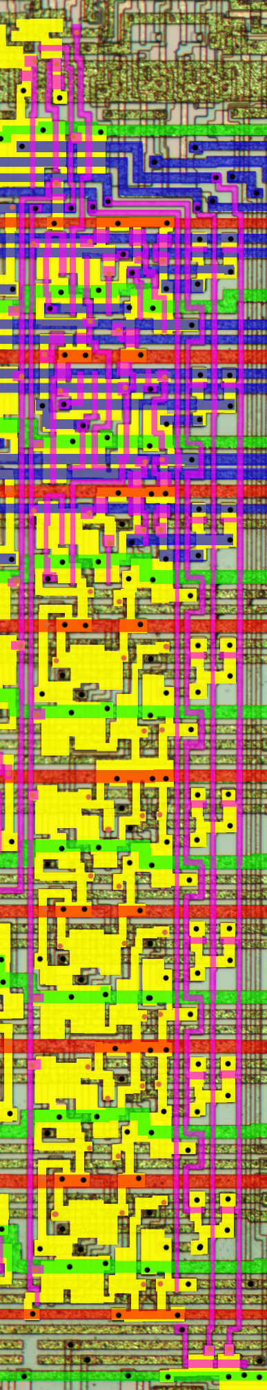
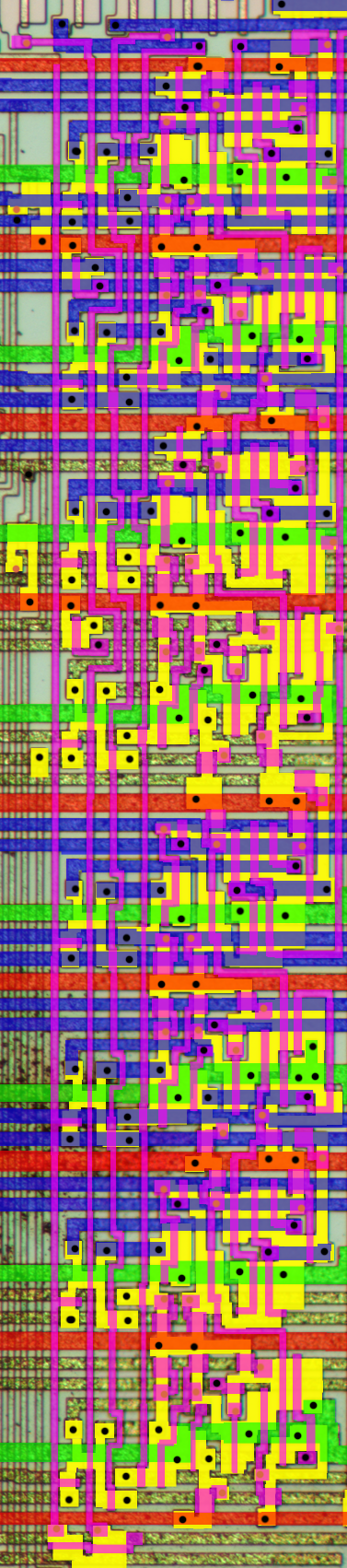
More progress on crazy logic :
Image no longer available: http://ogamespec.com/imgstore/whc4ffae6ac6ec5a.jpg
I began to understand how it works in general

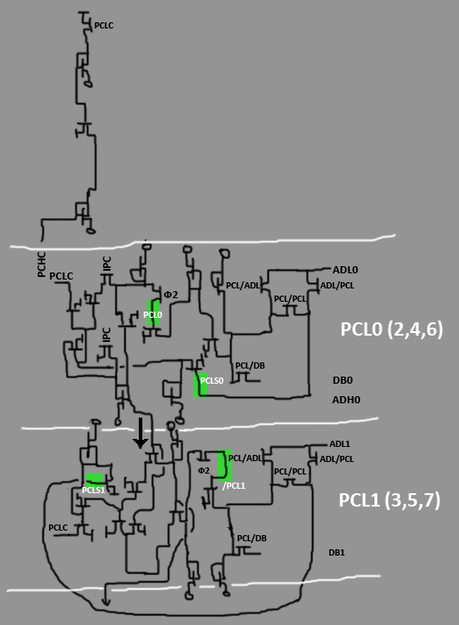
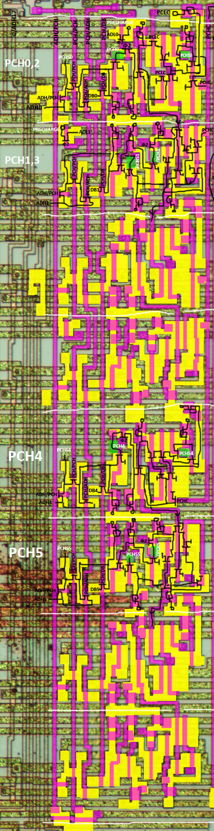
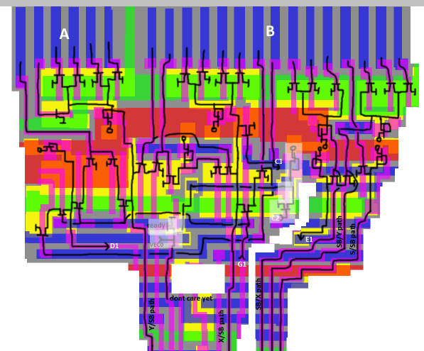
PLA outputs are joined in "groups".
Groups on the left works with X,Y and S registers (resided underneath).
Groups on the middle are ALU related, which feed its inputs.
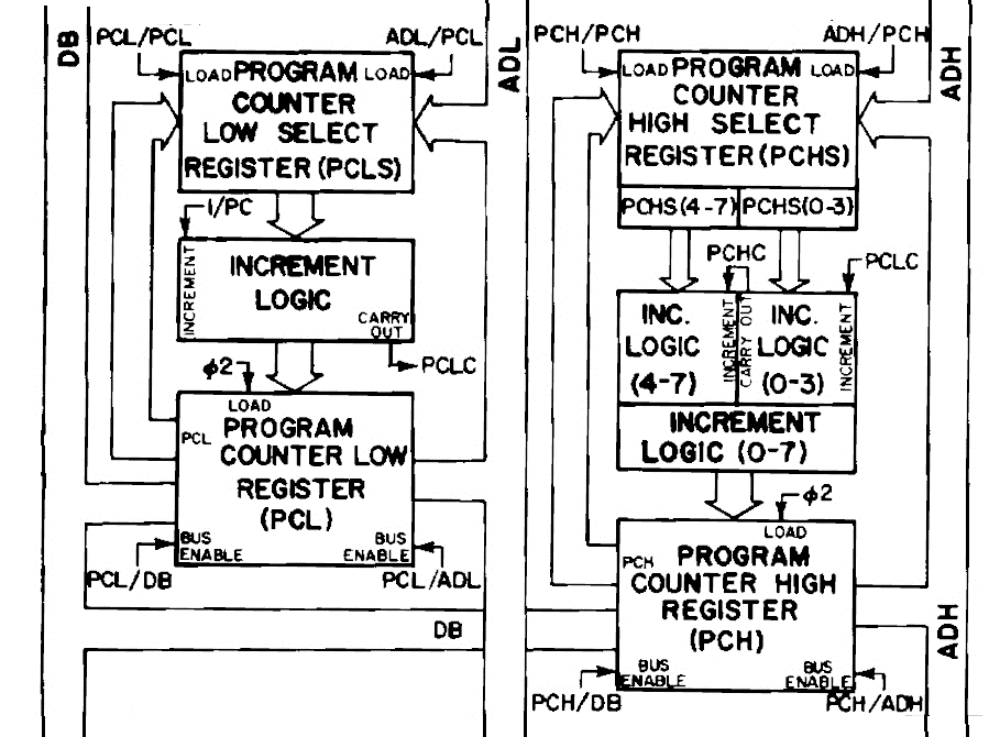
Groups on the right are branch/flag/compare and (possibly) interrupt/reset logic; instructions related to program counter (PC is resided on the bottom right side of the 6502).
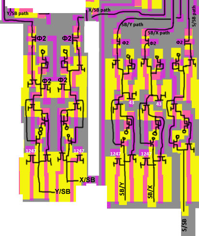
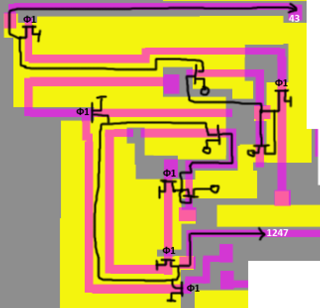
Also there is intense metall layer crosspassing from the left to the right, for addressing calculations purposes.
Hope to crunch it fast, when I get full color schematics (good for LSD trips BTW

)