
Do you need those RAM blocks to be so far apart in the memory space ?
It would simplify your schematic if you make a single RAM, located at 0000, but make it twice as big
A 6502 SoC Project using a Spartan 3 FPGA
-
ElEctric_EyE
- Posts: 3260
- Joined: 02 Mar 2009
- Location: OH, USA
It would be much simpler if I could use 1 48K or even 1 64K BRAM (and deselect when necessary), but anything above 32K and the number turned red indicating out of range for selected device.
The lower 16K is for 0 page/stack. The 32K is intended for the window into the 2M flash.
I will use a MUX, thanks! I'm curious to see how much resources all this will use once I get it to pass synthesis.
The lower 16K is for 0 page/stack. The 32K is intended for the window into the 2M flash.
I will use a MUX, thanks! I'm curious to see how much resources all this will use once I get it to pass synthesis.
The problem is that there's a limited amount of block RAM inside the device. I don't know which one you intend to use, but the capacity is as follows:
XC3S50 : 4 block RAMs
XC3S200: 12 block RAMs (I'm using this one)
XC3S400: 16 block RAMs
Each block RAM is 2kB big, so if you're using the XC3S400, you'll be limited to 32KB max, if you use all block RAMs. Of course, you will only have resources for one of those RAMs.
Since you already need 2 block RAMs for your ROM, you only have 14 left in the XC3S400 for your RAM, or 28kB max. Less if you want to use block RAMs for something else.
Your resource use will be mainly CPU+block RAM, plus a little bit for the select and the MUX. A 3-input MUX uses 2 LUTs per bit, or 16 LUTs total.
The 3-input OR uses only 1 LUT per bit, and will be faster as well.
If the flash is a parallel NOR flash, you don't really need a window + RAM. You can just map it directly on the 6502 memory bus through a async memory controller.
ETA: I just realized most flash is pretty slow, and you probably don't want to slow down the 6502 too much, by putting it directly on the 6502 bus. My 6502 core model doesn't support RDY signaling, so the clock rate should be lowered to match the flash. I guess RDY support could be added too, but I'm not sure how hard that is, and how many resources it would take.
A solution could be to make the RAM buffer a lot smaller, and a DMA controller that can copy arbitrary blocks of flash into arbitrary locations on the RAM.
-
ElEctric_EyE
- Posts: 3260
- Joined: 02 Mar 2009
- Location: OH, USA
Arlet wrote:
...Your resource use will be mainly CPU+block RAM, plus a little bit for the select and the MUX. A 3-input MUX uses 2 LUTs per bit, or 16 LUTs total.
The 3-input OR uses only 1 LUT per bit, and will be faster as well.
The 3-input OR uses only 1 LUT per bit, and will be faster as well.
Also, obviously I was not paying attention to the Block Ram datasheet... The ROM is the constant at this point, and can be no less than 4K. As you pointed out that leaves me with 28672 bytes. It would be nice to use an even chunk of memory for the window, which would leave 16384 bytes for the window, and 12288 for lower memory. If the ROM grows, the lower memory will shrink.
Arlet wrote:
...My 6502 core model doesn't support RDY signaling, so the clock rate should be lowered to match the flash...
-
ElEctric_EyE
- Posts: 3260
- Joined: 02 Mar 2009
- Location: OH, USA
Arlet wrote:
There are two options:...
2) Enable the SSR input on your memories. Tie enable input to '1', and attach inverted enable signal to SSR input. Asserting the SSR will produce a '0' on the douta signals. This way all the douta values will be zero, except for the one memory that you're addressing. Then use an 3-input OR to OR all douta wires together.
2) Enable the SSR input on your memories. Tie enable input to '1', and attach inverted enable signal to SSR input. Asserting the SSR will produce a '0' on the douta signals. This way all the douta values will be zero, except for the one memory that you're addressing. Then use an 3-input OR to OR all douta wires together.
So this is interesting that, because there is no internal tri-stating (except on the top-level I/O), all devices on the internal data bus are always enabled, if they are actively Reset they output "0"'s. If they are "enabled" by an inactive Reset, the device outputs its' data.
This is a totally different way of thinking for me, but it makes sense as there will be no bus contention like there would be if 2 discrete IC devices were output enabled simultaneously. In NMOS, this would have destroyed IC's. In CMOS, this would've locked up the system. In this type of setup however, you just get garbage info because all outputs or OR'd.
So thinking ahead to the PS2 core and I2C core that will have to communicate with the 6502 core (in addition to the RAM's and ROM), they have a wishbone interface and do have Reset's as well. I will have to find out what value they output during an active Reset.
-
ElEctric_EyE
- Posts: 3260
- Joined: 02 Mar 2009
- Location: OH, USA
One step closer to wirewrap....
The 3 30-pin connector's to the right of the ground plane (next to the 144-pin QFP adapter) will be replaced with 40-pin connectors as mentioned before (I just used them for spacing since I had them on hand, the 144-pin QFP is being used as a spacer too).
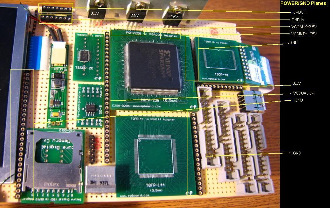
This is the first power "plane" in this wire wrap project. It is the ground plane. Mechanically, and soon to be electrically sound (soldered). Noise will be a very limited variable!.
All power planes will be connected with seamless 14AWG solid copper wire. The only IC shown is the XC3S400... (The 208-pin adapter is difficult to place into the perf-board, so I didn't try to remove it). I'm also looking into thicker wirewrap wire for power connections, currently using 30AWG for signalling.
The 3 30-pin connector's to the right of the ground plane (next to the 144-pin QFP adapter) will be replaced with 40-pin connectors as mentioned before (I just used them for spacing since I had them on hand, the 144-pin QFP is being used as a spacer too).
This is the first power "plane" in this wire wrap project. It is the ground plane. Mechanically, and soon to be electrically sound (soldered). Noise will be a very limited variable!.
All power planes will be connected with seamless 14AWG solid copper wire. The only IC shown is the XC3S400... (The 208-pin adapter is difficult to place into the perf-board, so I didn't try to remove it). I'm also looking into thicker wirewrap wire for power connections, currently using 30AWG for signalling.
-
ElEctric_EyE
- Posts: 3260
- Joined: 02 Mar 2009
- Location: OH, USA
I finished the Power/GND planes today...
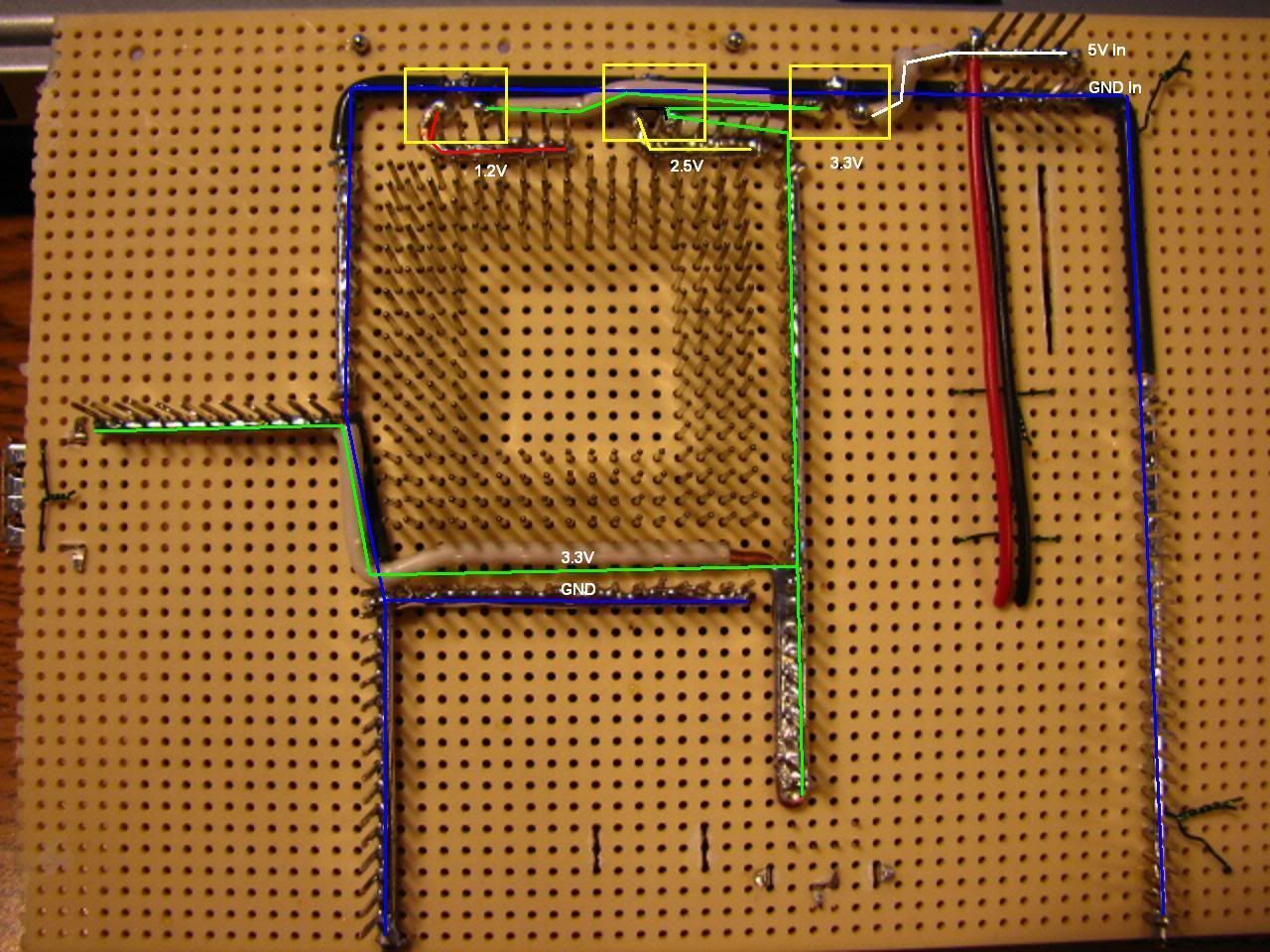
EDIT 2/9/11: Added GND plane below FPGA.
Rewired 1.2VReg for 3.3VIn instead of 2.5VIn
EDIT 2/9/11: Added GND plane below FPGA.
Rewired 1.2VReg for 3.3VIn instead of 2.5VIn
Last edited by ElEctric_EyE on Wed Feb 09, 2011 5:23 pm, edited 2 times in total.
-
GARTHWILSON

- Forum Moderator
- Posts: 8775
- Joined: 30 Aug 2002
- Location: Southern California
- Contact:
-
ElEctric_EyE
- Posts: 3260
- Joined: 02 Mar 2009
- Location: OH, USA
We shall see!
The 14AWG wires act like power/GND planes. I will tap into them when I wire in the power connections to the FPGA. Then add the bypass cap's...
I realize all this wirewrapping invites an inductive challenge and will limit top speed, but if I can achieve at least a working prototype then I will have a foundation from which to work from when it's time to design a professional 4 layer board.
EDIT: 14AWG not 24AWG.
Last edited by ElEctric_EyE on Wed Feb 09, 2011 1:55 pm, edited 1 time in total.
-
GARTHWILSON
- Forum Moderator
- Posts: 8775
- Joined: 30 Aug 2002
- Location: Southern California
- Contact:
Fairchild has an ap. note on ground bounce caused by ground inductance at https://www.onsemi.com/pub/Collateral/AN-640.pdf.pdf .
The inductance of the wire does not improve much by going from 30AWG WW wire to the 24AWG. There's a wire-inductance calculator at http://www.consultrsr.com/resources/eis/induct5.htm you can plug the numbers into. [Edit, 4/3/14: That domain seems to have expired. There's another online wire inductance calculator at http://www.eeweb.com/toolbox/wire-inductance/.] The only way to make it well behaved as a ground plane would be if you could wrap around it all the signal wires whose return current will flow through that ground wire, and they were small enough compared to its size that they could all be against the ground wire. Obviously not possible.
If it will work at all, it might work at whatever number of MHz the parts can go, if only the clock portion of the circuit is clean. The construction presents problems with rise time though, not MHz, and, with a given set of parts, the rise time may be just as bad to work with at 100kHz as they are at 100MHz.
Dr. Howard Johnson's relatively short answer to someone's wire-wrap question at https://web.archive.org/web/20120302190 ... ws/2_8.htm may be helpful.
You can get perfboard with a ground plane which will improve things a lot even if you still use WW. Still, put the parts as close together as possible to keep connections as short as possible.
http://WilsonMinesCo.com/ lots of 6502 resources
The "second front page" is http://wilsonminesco.com/links.html .
What's an additional VIA among friends, anyhow?
The "second front page" is http://wilsonminesco.com/links.html .
What's an additional VIA among friends, anyhow?
-
ElEctric_EyE
- Posts: 3260
- Joined: 02 Mar 2009
- Location: OH, USA
Thanks for pointing out those articles Garth (I've bookmarked his site, lots of good info in there!), especially the wire-wrap question! Good to see I am not the only one using wirewrap for prototyping. Dr. Johnson theorized a top speed of 33MHz, but I'm sure that was for a complicated system. I've run 16-bit counters inside a spartan 2 @80MHz in the PWA successfully. I paid close attention to bypassing all power pins, but I used a similar but more primitive approach to using power/ground "planes" with 24AWG. They were for a MUCH smaller 100-pin QFP package though...
The idea behind the power bars (I'll call them "bars" from now on since they are not technically planes), is to be able to tap a voltage from a single point. The thicker the wire, the closer you come to that single point, though it may be 5 inches away from the source. With so many power pins and grounds coming out of that beautiful 208-pin monstrosity, not to mention the bypass caps I'll have to wire in, I used the thickest AWG I could get my hands on!
After doing some reading on DCM's (yes I'm only up to Chap 3) in the Spartan 3 User Guide, I realized I am doing a no-no by cascading the voltage regulators (Pg.148). It mentions that if this situation is unavoidable, then every VCCAUX must be bypassed which I was intending to do anyway.
I looked at a schematic for a Spartan 3 starter board from Digilent. They have the VCCO regulator feeding both VCCAUX and VCCINT regulators. I have changed my wiring to be the same.
Also, I have added one more ground bar underneath the Spartan 3. The 144-pin QFP adapter is right on the bottom edge, but it still fits! I'll edit the last pic soon, as now there are 2 major finalizations.
Today and tomorrow I am off from work, my little hands will be busy! Now thinking about it (typing helps me think clearer), I should wire the power and grounds, then wire in JTAG and see if ISE recognizes the FPGA, before I wire all the bypass cap's. This will give me confidence and potentially save alot of rewiring in case I get double vision and wire a wrong pin. All those cap's are gonna get messy.
-
ElEctric_EyE
- Posts: 3260
- Joined: 02 Mar 2009
- Location: OH, USA
Speaking of JTAG, I almost forgot I'm using a serial config PROM in Master Serial mode. I'm new to this, but this much I have gathered from the Spartan 3 Configuration Guide on Pg.82, the associated appnote and the Digilent schematic mentioned b4.
I am unsure what to do about the resistor from VCCAUX(2.5V) regulator to GND mentioned in the appnote (R7 below, when the pic updates...). The value there is ~240ohms. In the Digilent schematic it is a 2.2K resistor?!...
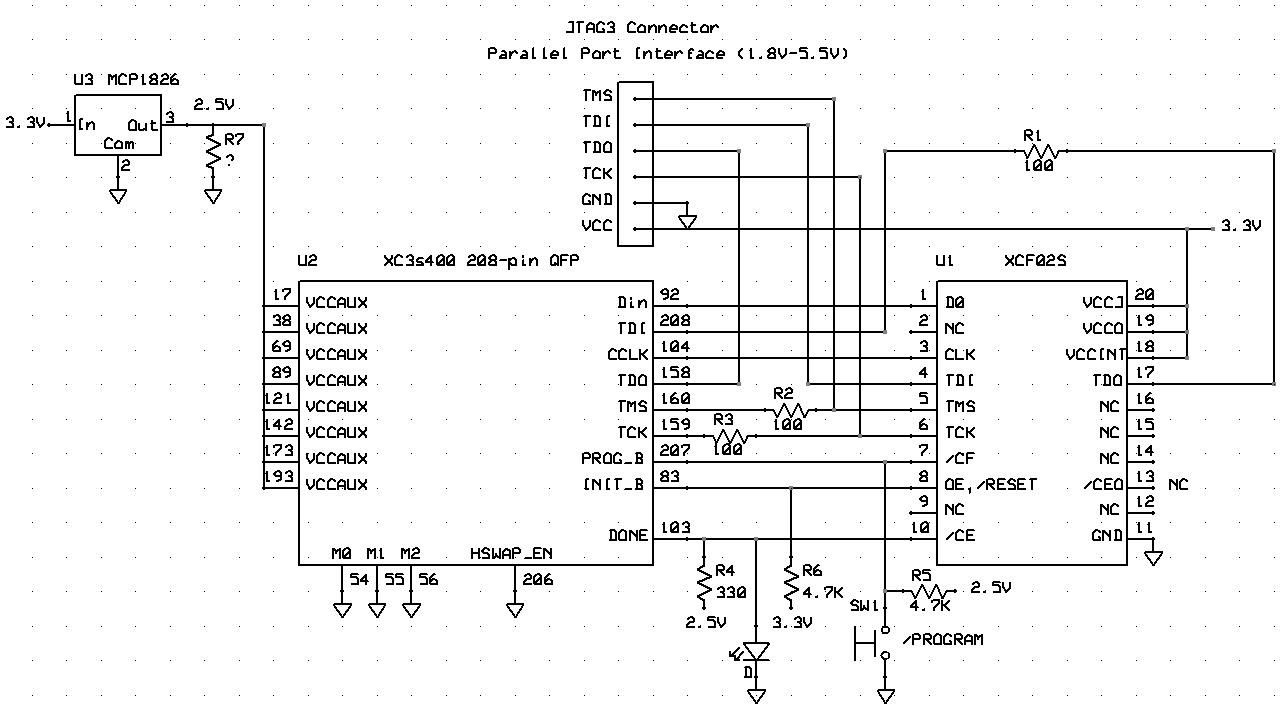
I am unsure what to do about the resistor from VCCAUX(2.5V) regulator to GND mentioned in the appnote (R7 below, when the pic updates...). The value there is ~240ohms. In the Digilent schematic it is a 2.2K resistor?!...
-
ElEctric_EyE
- Posts: 3260
- Joined: 02 Mar 2009
- Location: OH, USA
GARTHWILSON wrote:
...The inductance of the wire does not improve much by going from 30AWG WW wire to the 24AWG...
Digikey had a 100' spool for $15 and a 24AWG WW sleeve for $35. Found a 24AWG WW bit on ebay for $11.
I was thinking of using the 24AWG for the bypass caps as well, but after thinking about your post Garth, it makes sense to stay with 30AWG for the cap's, as well as staying with .1uF bypass cap's I've successfully used in the PWA project thanks to your suggestions.