JSR Abs is both fun and irritating. It's enlightening to see how they conserved resources by shuffling data all around the chip, but it also means I have to implement a large number of control signals before JSR Abs works
6502 Timing Controls: T0?
Quick progress update. I got LDA # (opcode A9) working, and am putting in all the logic needed for JSR Abs.
JSR Abs is both fun and irritating. It's enlightening to see how they conserved resources by shuffling data all around the chip, but it also means I have to implement a large number of control signals before JSR Abs works Luckily the bus control signals are pretty simple. The ALU controls might prove a bit more difficult ...
JSR Abs is both fun and irritating. It's enlightening to see how they conserved resources by shuffling data all around the chip, but it also means I have to implement a large number of control signals before JSR Abs works

As far as I know, the flip flop blocks inside the FPGA can be configured as latches, so it should work, However, the tools and the hardware are optimized for flip flops, not for latches, so for large designs with latches you're probably in uncharted terrority 
I've never used latches, except by accident.
I've never used latches, except by accident.

Excellent! I'm not sure how much care and knowledge went into the default program on visual6502, but I think it might exercise quite a few difficult cases - difficult for the switch-level model doesn't necessarily mean difficult for an HDL model of course.
On the subject of latches and clocking, here's a thing: when the 6502 fetches a second operand byte which appears on the high address byte in the very next phase, you'll find that there's a phi2 latch to capture the databus into the IDL, and then in phi1 the data actually has to pass through 2 phi1 latches - and cross quite a distance - to appear on the databus at the beginning of the next cycle. (I was naively expecting that successive latches would always alternate between the two phases.) This will be why it takes some time for the address bus to become valid at the beginning of the cycle.
Here's a simulation which stops on the phase in question, and here's a URL which highlights the signals involved in getting from DB3 to AB11. (The simulation shows activity only per phase so you can't see the gate-by-gate information flow.)
Here's a shorter simulation to illustrate how to change the program using the URL and to put a more distinctive value on the bus.
Cheers
Ed
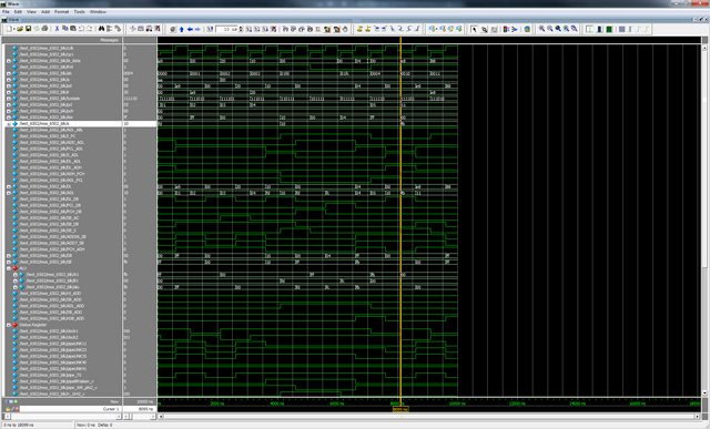
Edit: thumbnail of a screenshot
On the subject of latches and clocking, here's a thing: when the 6502 fetches a second operand byte which appears on the high address byte in the very next phase, you'll find that there's a phi2 latch to capture the databus into the IDL, and then in phi1 the data actually has to pass through 2 phi1 latches - and cross quite a distance - to appear on the databus at the beginning of the next cycle. (I was naively expecting that successive latches would always alternate between the two phases.) This will be why it takes some time for the address bus to become valid at the beginning of the cycle.
Here's a simulation which stops on the phase in question, and here's a URL which highlights the signals involved in getting from DB3 to AB11. (The simulation shows activity only per phase so you can't see the gate-by-gate information flow.)
Here's a shorter simulation to illustrate how to change the program using the URL and to put a more distinctive value on the bus.
Cheers
Ed
Edit: thumbnail of a screenshot
Quote:
On the subject of latches and clocking, here's a thing: when the 6502 fetches a second operand byte which appears on the high address byte in the very next phase, you'll find that there's a phi2 latch to capture the databus into the IDL, and then in phi1 the data actually has to pass through 2 phi1 latches - and cross quite a distance - to appear on the databus at the beginning of the next cycle.
Progress update: I've gotten through most of JSR Abs; just 3 more control signals need to be implemented. In fact, one of them is DL/ADH
Quote:
I've never used latches, except by accident.
Anyway, it's fun to learn about these "old" techniques they used in designing chips like the 6502.
EDIT:
I wrote this:
Quote:
Side Note: Weird thing I've noticed is that it appears as if some signals are controlled by inverted clocks. It's hard for me to tell for certain, since I mostly just tear apart the verilog to get to the functional design, ignoring any 100% electrical accuracy.
Now, from what I understand, the two clocks are exact opposites, they have small gaps in-between their edges. So if a latch were controlled by, for example, !phi1, it would actually begin latching before phi2 really begins. The latches controlling ADH, for example, seem to have this property.
Or I am be reading the verilog all wrong
Code: Select all
always @(posedge eclk) dpc30_ADHPCH_v <= cp1_v & !cclk_v & !n_1162_v;Looks like I finally got JSR Abs working. It seems to be more or less correct (ADL is incorrect for one cycle, but doesn't effect anything; possibly other things like that).
2 instructions down, 7 more to go before the visual6502 demo works.
Code:
2 instructions down, 7 more to go before the visual6502 demo works.
Code:
Code: Select all
`timescale 1ns/1ns

module mos_6502(clk, RW, ab, bi_data, cclk, cp1);

	input clk;
	inout [7:0] bi_data;	// Bi-directional data port
	output reg [15:0] ab = 16'h0000;	// Address
	output reg RW = 1'b1;		// data port direction. Low for data coming into the 6502, high for data going out.
	output reg cclk, cp1;


	reg [7:0] a = 8'hAA;	// Accumulator
	reg [7:0] s = 8'hFD;	// Stack pointer
	reg [7:0] pd = 8'h00;	// Pre-decode Register
	reg [7:0] ir = 8'h00;	// Instruction Register
	reg [5:0] tcstate = 6'b111111;		// Timing Control
	reg [7:0] pcl = 8'h00, pch = 8'h00;	// Program Counter Low and High
	reg [7:0] dor = 8'h00;		// Data Output Register
	reg [7:0] B1 = 8'h00;		// B Input Register (used by ALU)
	reg [7:0] A1 = 8'hFF;		// A Input Register (used by ALU)
	reg [7:0] alu = 8'h00;		// alu result
	reg [7:0] DL = 8'h00;	// Data Latch (DL)

	reg ADL_ABL = 1'b1;	// Load ADL into Address Bus Register Low
	reg I_PC = 1'b0;	// Increment Program Counter

	// Address Low Bus
	reg ADD_ADL = 1'b1, PCL_ADL = 1'b0, S_ADL = 1'b0, DL_ADL = 1'b0;	// Flags that select the source for Address Data Low (ADL)
	wire [7:0] ADL = S_ADL ? s : (PCL_ADL ? pcl : (DL_ADL ? DL : (ADD_ADL ? alu : 8'hFF)));

	reg d_0ADH17 = 1'b0;
	reg PCH_ADH = 1'b0;
	reg ADH_ABH = 1'b1;
	reg ADH_PCH = 1'b1;
	reg DL_ADH = 1'b1;
	reg ADL_PCL = 1'b1;

	// Address High Bus
	wire [7:0] ADH = d_0ADH17 ? 8'h01 : (PCH_ADH ? pch : (DL_ADH ? DL : 8'hFF));

	reg DL_DB = 1'b1;	// Connect DL to DB
	reg PCL_DB = 1'b0;	// Connect PCL to DB
	reg PCH_DB = 1'b0;	// Connect PCH to DB
	reg SB_DB = 1'b0;	// Connect SB and DB
	reg ADD06_SB = 1'b0;	// Connect alu[6:0] to SB[6:0]
	reg ADD7_SB = 1'b0;	// Connect alu[7] to SB[7]
	reg SB_AC = 1'b0;	// Store SB into Accumulator
	reg SB_S = 1'b0;	// Store SB into Stack pointer

	// TODO: These busses might need to be setup as bidirectional, since
	// SB_DB is a two-way connection. We'll see. The following just
	// simulates bi-directionality.
	reg [7:0] DB;	// Data Bus (DB)
	reg [7:0] SB;	// Second Bus (SB)	// TODO: Is it Second Bus? Or South Bus? Or Sexy Bus!?
	always @*
	begin
		DB = 8'hzz;
		SB = 8'hzz;

		if(DL_DB)
			DB = DL;
		else if(PCL_DB)
			DB = pcl;
		else if(PCH_DB)
			DB = pch;

		if(ADD06_SB | ADD7_SB)
			SB = {ADD7_SB ? alu[7] : 1'b1, ADD06_SB ? alu[6:0] : 7'b1111111};

		if(SB_DB && (DB !== 8'hzz || SB !== 8'hzz))
		begin
			if(SB !== 8'hzz)
				DB = SB;
			else
				SB = DB;
		end
		else
		begin
			if(DB === 8'hzz)
				DB = 8'hFF;	// Float High
			if(SB === 8'hzz)
				SB = 8'hFF;	// Float High
		end
	end


	// ALU Load Flags
	reg DB_ADD = 1'b0;
	reg nDB_ADD = 1'b0;	// Load Inverted DB into B1
	reg SB_ADD = 1'b0;
	reg ADL_ADD = 1'b0;
	reg r0_ADD = 1'b0;	// Load 0 into A1


	assign bi_data = (!RW & cclk) ? dor : 8'bzzzzzzzz;


	// Status Register
	reg p0 = 1'b0, p1 = 1'b1, p2 = 1'b1, p3 = 1'b0, p4 = 1'b1, p6 = 1'b0, p7 = 1'b0;

	wire clock1 = tcstate[0], clock2 = tcstate[1];


	// cclk domain
	reg pipeUNK11 = 1'b0, pipeUNK23 = 1'b0, pipeUNK34 = 1'b1, pipeUNK35 = 1'b0, pipeUNK40 = 1'b0, pipeUNK41 = 1'b1, pipe_T0 = 1'b0, pipeBRtaken_v = 1'b0, pipe_WR_phi2_v = 1'b1;
	reg n_1505_v = 1'b1, n_521_v = 1'b1, n_1477_v = 1'b1, n_1027_v = 1'b1, n_360_v = 1'b0;
	reg not265 = 1'b1, not1162 = 1'b1;

	// cp1 domain
	reg n_24_v = 1'b1, n_653_v = 1'b0, n_666_v = 1'b0, n_1338_v = 1'b0;

	reg shifted_clk;
	always #100 shifted_clk = clk;

	always @ (posedge shifted_clk) cclk <= 1'b1;
	always @ (negedge clk) cclk <= 1'b0;

	always @ (negedge shifted_clk) cp1 <= 1'b1;
	always @ (posedge clk) cp1 <= 1'b0;


	/////////////////////////////////////////////////////////////////
	// Pre-Decoder
	wire fetch_v = pipeUNK11;
	wire clearIR = !fetch_v;

	wire [7:0] pd_clearIR = clearIR ? 8'd0 : pd;

	wire PD_xxxx10x0_v = !(pd_clearIR[0] | !pd_clearIR[3] | pd_clearIR[2]);
	wire PD_1xx000x0_v = !(!pd_clearIR[7] | pd_clearIR[0] | pd_clearIR[3] | pd_clearIR[4] | pd_clearIR[2]);
	wire PD_0xx0xx0x_v = !(pd_clearIR[7] | pd_clearIR[4] | pd_clearIR[1]);
	wire PD_xxx010x1_v = !(!pd_clearIR[3] | pd_clearIR[4] | !pd_clearIR[0] | pd_clearIR[2]);
	wire PD_n_0xx0xx0x_v = !PD_0xx0xx0x_v;

	wire TWOCYCLE = (PD_n_0xx0xx0x_v & PD_xxxx10x0_v) | (PD_1xx000x0_v | PD_xxx010x1_v);
	/////////////////////////////////////////////////////////////////


	// PLA
	// TODO: This should be a module that takes the appropriate inputs and
	// gives a large 130 bit output. We can then write an include that
	// assigns named wires to the bit array.
	`include "pla_decode.v"


	wire n_256_v = ~((op_T5_ind_x_v|op_T0_brk_rti_v|op_T0_jmp_v|op_T5_rts_v|op_T4_v|op_T5_rti_v|op_T3_v));
	wire n_347_v = ~((op_T2_mem_zp_v|op_T3_mem_zp_idx_v|op_T3_mem_abs_v|op_T4_mem_abs_idx_v|op_T5_mem_ind_idx_v));
	wire n_790_v = ~((op_asl_rol_v|op_lsr_ror_dec_inc_v));
	wire n_368_v = ~((x_op_T3_plp_pla_v|op_T2_jmp_abs_v|op_T4_jmp_v|op_T5_rti_rts_v|xx_op_T5_jsr_v|op_T2_php_pha_v));
	wire n_1455_v = ~((op_T__shift_a_v|op_T0_lda_v|op_T__adc_sbc_v|op_T0_tya_v|op_T__ora_and_eor_adc_v|op_T0_pla_v|op_T0_txa_v));


	wire n_1716_v = ~(op_T3_branch_v | n_653_v | !n_368_v);
	wire n_1286_v = ~(op_brk_rti_v | x_op_jmp_v | op_jsr_v | clock1);
	wire n_1211_v = ~(op_T5_jsr_v | op_T2_branch_v | n_1286_v | !n_666_v | op_T2_abs_access_v);
	wire n_182_v = clock1 & !op_T5_rts_v & n_1211_v;
	wire n_1619_v = !(op_T2_branch_v | n_182_v);
	wire n_620_v = (_op_branch_bit7_v | _op_branch_bit6_v | !p1) & (!p0 | !_op_branch_bit6_v | _op_branch_bit7_v);
	wire BRtaken_v = (ir[5] | !(_op_branch_bit7_v | _op_branch_bit6_v | !p1) ) & (!ir[5] | n_620_v);

	wire n_335_v = !(_op_store_v | n_347_v);
	wire n_844_v = !(op_T__dex_v | op_T0_ldx_tax_tsx_v | op_T__inx_v);
	wire n_616_v = !(op_T0_tay_ldy_not_idx_v | op_T0_ldy_mem_v | op_T__iny_dey_v);
	wire n_946_v = !(n_844_v & n_616_v);
	wire n_384_v = !(n_653_v | n_946_v | !n_1455_v | op_ANDS_v);
	wire n_550_v = !(n_384_v | op_ANDS_v);
	wire n_905_v = n_24_v | !op_shift_v;
	wire n_1107_v = ~(((!n_24_v&op_inc_nop_v)|(op_plp_pla_v|op_T3_ind_x_v|op_T4_ind_y_v|op_T3_abs_idx_v|op_T2_ind_y_v)));
	wire n_275_v = (op_T2_abs_access_v|!clock1) & !op_implied_v;
	wire n_272_v = ~((!n_666_v|op_T2_abs_access_v|op_T2_branch_v|!clock1|op_T3_branch_v|op_T5_rts_v));
	wire n_1642_v = n_1338_v | op_T3_jsr_v | op_T2_brk_v;
	wire n_1109_v = op_T3_plp_pla_v|op_T5_rti_v|op_T0_php_pha_v|op_T0_jsr_v|op_T4_rts_v|op_T5_brk_v;
      	wire n_1130_v = ~((n_653_v|n_1109_v|op_T5_jsr_v|!n_666_v));


	always @ (posedge cclk)
	begin
		pipeUNK11 <= !n_666_v;
		pipeUNK23 <= clock1;
		pipeUNK34 <= !(op_T3_jsr_v | op_T2_brk_v);
		pipeUNK35 <= n_1716_v & clock1;
		pipeUNK40 <= !(n_790_v | n_347_v);
		pipeUNK41 <= n_24_v;

		pipe_T0 <= clock1;
		pipeBRtaken_v <= !(n_1619_v | (BRtaken_v & op_T2_branch_v));
		pipe_WR_phi2_v <= ~((op_T2_php_pha_v|n_653_v|op_T4_brk_v|!n_24_v|~(_op_store_v|n_347_v)|n_1642_v));
		n_1505_v <= n_1455_v;
		n_521_v <= ~(op_T3_plp_pla_v|op_T5_rti_v|op_T0_php_pha_v|op_T0_jsr_v|op_T4_rts_v|op_T5_brk_v | op_T0_txs_v | op_T2_jsr_v);
		n_1477_v <= ~(((op_T2_ADL_ADD_v&!op_T0_v)|(op_T3_ind_x_v|op_T3_stack_bit_jmp_v|op_T2_stack_v|op_T4_brk_jsr_v|op_T4_rti_v)));
		n_1027_v <= ~((!n_1107_v|op_T4_ind_x_v|op_rti_rts_v|op_jmp_v|op_T2_jsr_v|op_T2_abs_v|op_T3_plp_pla_v|op_T5_rti_v|op_T0_php_pha_v|op_T0_jsr_v|op_T4_rts_v|op_T5_brk_v));
		n_360_v <= !n_1107_v|op_T4_ind_x_v|op_rti_rts_v|op_jmp_v|op_T2_jsr_v|op_T2_abs_v|op_T3_plp_pla_v|op_T5_rti_v|op_T0_php_pha_v|op_T0_jsr_v|op_T4_rts_v|op_T5_brk_v;
		not265 <= !clock1 | op_T5_rts_v | !n_1211_v | op_T3_branch_v;
		not1162 <= !n_666_v | op_T2_abs_access_v | op_T2_branch_v | !clock1 | op_T3_branch_v | op_T5_rts_v;
		nDB_ADD <= op_T0_cmp_v|op_T0_cpx_cpy_inx_iny_v|op_T0_sbc_v|op_T5_jsr_v;		// !805

		pd <= bi_data;

		DL <= bi_data;


		// Bus Control Signals
		ADL_ABL <= !n_653_v & n_24_v;
		ADD_ADL <= !n_256_v;
		PCL_ADL <= op_T5_jsr_v | op_T2_branch_v | op_T2_abs_access_v | ( !( op_brk_rti_v | x_op_jmp_v | op_jsr_v ) & !clock1 ) | !n_666_v;
		S_ADL <= op_T2_stack_v | op_T0_jsr_v;
		DL_ADL <= op_T2_ind_v | op_T2_zp_zp_idx_v;

		SB_DB <= op_T2_jsr_v | (op_sty_cpy_mem_v & n_335_v) | (op_from_x_v & n_335_v) | n_550_v | op_T0_shift_a_v | op_T2_branch_v | !n_905_v | !n_666_v;
		DL_DB <= op_T2_branch_v | op_T4_jmp_v | op_T2_jsr_v | x_op_T3_ind_y_v | op_T4_ind_x_v | !n_1107_v | op_rti_rts_v | n_275_v | !n_24_v;
		PCL_DB <= n_1338_v;
		PCH_DB <= op_T3_jsr_v|op_T2_brk_v;

		d_0ADH17 <= op_T2_ind_v | op_T2_zp_zp_idx_v | op_T2_stack_access_v;
		ADH_ABH <= op_T2_v | x_op_T4_ind_y_v | op_T3_abs_idx_ind_v | op_T5_rts_v | op_T5_ind_x_v | !n_272_v | op_T5_jsr_v;
		ADD06_SB <= !n_1130_v;
		ADD7_SB <= !n_1130_v;
		PCH_ADH <= !(op_branch_done_v|n_1211_v|((op_brk_rti_v|x_op_jmp_v|op_jsr_v)&!clock1));
		DL_ADH <= ((op_brk_rti_v | x_op_jmp_v | op_jsr_v) & !clock1) | x_op_T4_ind_y_v | op_T3_abs_idx_ind_v | op_T5_rts_v | op_T5_ind_x_v;


		// ALU
		alu <= A1 + B1;		// Most advanced ALU of all time.
	end


	always @ (posedge cp1)
	begin
		n_24_v <= !pipeUNK40;
		n_653_v <= !pipeUNK41;
		n_666_v <= pipeUNK23;
		n_1338_v <= !pipeUNK34;

		if(ADL_ABL)
			ab[7:0] <= ADL;
		if(ADH_ABH)
			ab[15:8] <= ADH;

		dor <= DB;
		RW <= pipe_WR_phi2_v;

		SB_AC <= !n_1505_v;

		// Store SB into Accumulator
		if(!n_1505_v)
			a <= SB;

		// Increment PC?
		I_PC <= pipeBRtaken_v | PD_xxxx10x0_v;

		ADH_PCH = not1162;
		ADL_PCL = not265;

		if(!(pipeBRtaken_v | PD_xxxx10x0_v))
			{pch, pcl} <= {(ADH_PCH ? ADH : pch), (ADL_PCL ? ADL : pcl)} + 16'd1;

		SB_S <= !n_521_v;

		if(!n_521_v)
			s <= SB;

		ADL_ADD <= !n_1477_v;

		if(!n_1477_v)
			B1 <= ADL;
		else if(nDB_ADD)
			B1 <= ~DB;

		// 0ADD
		if(!n_1027_v)
			A1 <= 8'h00;

		// SB_ADD
		if(!n_360_v)
			A1 <= SB;

		if(fetch_v)
			ir <= pd_clearIR;

		// Timing Control
		tcstate[0] <= (pipeUNK35 & !TWOCYCLE) | !pipe_T0;
		tcstate[1] <= pipe_T0;
		tcstate[2] <= tcstate[1];

		if(!pipeUNK35)
			tcstate[5:3] <= 3'b111;
		else
			tcstate[5:3] <= tcstate[4:2];
	end

endmodule
YAY! It looks like I've gotten the full visual6502 example program running! There are still 27 control signals left unimplemented; they aren't exercised by the simple example program. Nevertheless, I'm happy to have something running.
I guess the next step is to find examples on 6502asm.com that exercise the other control signals and get those programs running.
I should also be able to synthesize soon, and see some of those 6502asm.com examples running on a real FPGA with glorious 32x32 displayed on an HDTV.
Should I put this project on github or something like that? The code is a bit messy as is...
-
ElEctric_EyE
- Posts: 3260
- Joined: 02 Mar 2009
- Location: OH, USA
Xor wrote:
Should I put this project on github or something like that? The code is a bit messy as is...
With the code on github, it's easy to link to specific files and possibly even specific lines if you want to discuss. A forum thread is good for project updates and discussions.
Xor wrote:
Aren't those two groups of phi1 latches the ones controlled by DL/ADH and ADH/ABH?
Cheers
Ed
-
GARTHWILSON

- Forum Moderator
- Posts: 8774
- Joined: 30 Aug 2002
- Location: Southern California
- Contact:
continued here