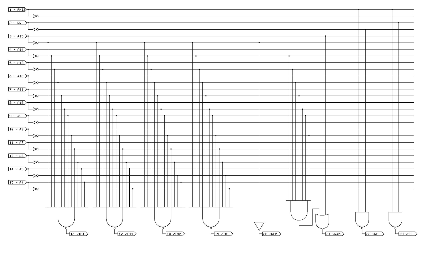
It consists of a 24 pin 0.3" wide DIP Lattice 22V10 GAL chip programmed to provide chips selects to a 32K ROM, 32K SRAM, and four IO Devices. It will also take the RW and PHI2 pins from the 6502/65816 and produce a /OE and /WE signal for the memories.
This one chip can be used to replace several standard logic chips and also provides flexibility in assigning IO addresses.
The standard map will look like this:
Code: Select all
$0000-$01FF - RAM
$0200-$020F - IO Device #1 (16 bytes)
$0210-$021F - IO Device #2 (16 bytes)
$0220-$022F - IO Device #3 (16 bytes)
$0230-$023F - IO Device #4 (16 bytes)
$0240-$02FF - unassigned (can be externally decoded for use)
$0300-$7FFF - RAM
$8000-$FFFF - ROM
Options include adding a second RAM chip select to allow for more RAM and less ROM, i.e. 48K RAM and 16k ROM.
The propagation delay is 10ns.
Here is the pinout for the standard configuration:
Code: Select all
       --------
PHI2  |1     24| Vcc
RW    |2     23| /OE
A15   |3     22| /WE
A14   |4     21| /RAM
A13   |5     20| /ROM
A12   |6     19| /IO1
A11   |7     18| /IO2
A10   |8     17| /IO3
A9    |9     16| /IO4
A8    |10    15| A4
A7    |11    14| A5
Gnd   |12    13| A6
--------For those with programmers, I will make the source code available soon.
Contact me for more info.
Daryl