6502.org Forum  Projects  Code  Documents  Tools  Forum
It is currently Wed May 08, 2024 9:07 am

All times are UTC


Post new topic Reply to topic  [ 86 posts ]  Go to page Previous  1, 2, 3, 4, 5, 6  Next
Author Message
 Post subject:
PostPosted: Tue Oct 12, 2010 6:53 pm 
Offline
User avatar

Joined: Thu Dec 11, 2008 1:28 pm
Posts: 10800
Location: England
Hi Garth
Michael Steil says that the normal interrupt sequence is followed - there are three stack accesses - but that RnW stays high, so there are no writes.
Do you believe you saw writes, or did you just see the addresses?
(I'm interested in this because I want to trace the part of the design which adjusts RnW.)
Cheers
Ed
ps. I'm not sure yet I agree with his statement "When a 6502 is turned on, the stack pointer is initialized with zero." but I haven't yet run this case through visual6502.


Top
 Profile  
Reply with quote  
 Post subject:
PostPosted: Tue Oct 12, 2010 7:32 pm 
Offline
User avatar

Joined: Fri Aug 30, 2002 1:09 am
Posts: 8432
Location: Southern California
Quote:
Michael Steil says that the normal interrupt sequence is followed - there are three stack accesses - but that RnW stays high, so there are no writes.
Do you believe you saw writes, or did you just see the addresses?

I'm sure I saw writes (ie, R/W\ was low) but I'd have to dig it up to be more than 90% sure.  The WDC manual also says they are writes, with R/W\ low.

Quote:
ps. I'm not sure yet I agree with his statement "When a 6502 is turned on, the stack pointer is initialized with zero."

In school in 1982 we were taught to always initialize it in the reset routine.  That was on the NMOS 6502 but what I find in WDC's data sheet is "All Registers are initialized by software except the Decimal and Interrupt disable mode select bits of the Processor Status Register (P) [which] are initialized by hardware." (page 11).  IOW, your reset routine has to initialize all but the D and I flags.

If you leave the entire page 1 of a 6502 for the stack, it wouldn't really matter if you initialize it, because there won't be anything to overwrite; but my own tests have shown that I don't need anywhere near that much stack space even with heavy use of subroutines and interrupts; so I use some of page 1 for variables and of course the stack must be kept in its place to avoid stepping on them.  [Edit, years later: There is another good reason to initialize the stack pointer, which is to make sure you don't accidentally index into page 2 if the stack wraps.  More on this in my stacks treatise, starting in the middle of page 4 on stack addressing, at http://wilsonminesco.com/stacks/stackaddressing.html .]

_________________
http://WilsonMinesCo.com/ lots of 6502 resources
The "second front page" is http://wilsonminesco.com/links.html .
What's an additional VIA among friends, anyhow?


Top
 Profile  
Reply with quote  
 Post subject:
PostPosted: Tue Oct 12, 2010 7:39 pm 
Offline
User avatar

Joined: Thu Dec 11, 2008 1:28 pm
Posts: 10800
Location: England
Thanks for that - it sounds like WDC added some initialisation hardware and subtracted a bit of reset-being-non-destructive hardware!

Cheers
Ed


Top
 Profile  
Reply with quote  
 Post subject:
PostPosted: Tue Oct 12, 2010 8:20 pm 
Offline
User avatar

Joined: Fri Aug 30, 2002 1:09 am
Posts: 8432
Location: Southern California
BTW, when I did my single-cycling test mentioned above, that was on a Rockwell 65c02, not WDC, but it agreed with WDC's data sheet.

_________________
http://WilsonMinesCo.com/ lots of 6502 resources
The "second front page" is http://wilsonminesco.com/links.html .
What's an additional VIA among friends, anyhow?


Top
 Profile  
Reply with quote  
 Post subject:
PostPosted: Tue Oct 12, 2010 9:56 pm 
Offline

Joined: Thu Sep 02, 2010 12:34 am
Posts: 36
Location: Salzburg, Austria
GARTHWILSON wrote:
I'm sure I saw writes (ie, R/W\ was low) but I'd have to dig it up to be more than 90% sure. The WDC manual also says they are writes, with R/W\ low.

Very interesting, thanks for the info!

After Michael's blog post I was very interested about seeing this in action so I hooked up my logic analyzer to my Atari 800XL and captured some traces.

Unfortunately Antic dram refreshes destroy the nice pics, just ignore all cycles where HALT is low (in the pics I shifted halt by 400ns so that it's in sync with the stopped clock cycles). To make the actual CPU cycles easier to recognize I set a marker at the start of each CPU cycle.

Here's the powerup:
Image


And here's the reset:
Image

I hope that I'm able to capture traces of the 65C02 in a few weeks, a friend was so kind to send me a few 65C02s, now I only need the adapter board.

so long,

Hias


Top
 Profile  
Reply with quote  
 Post subject:
PostPosted: Wed Oct 13, 2010 4:23 am 
Offline
User avatar

Joined: Thu May 28, 2009 9:46 pm
Posts: 8176
Location: Midwestern USA
digidice wrote:
there is a 74F138 but no 74ABT138

Correct on that. Not all parts will be available in all logic families. That was why I suggested ABT, F, AC.

Quote:
#5 A AND gate from /Ø2 and RWB to the /WE on the SRAM? That should qualify?

Naw, your logic will be upside down. Connect Ø2 to one input of a 74ABT00 NAND. Connect RWB to an inverter (74ABT04, for example) and connect the inverter's output to the other input of the 74ABT00. The 'ABT00 output will go low when Ø2 is high and RWB is low. The slight prop delay of the inverter won't matter because RWB will be low before Ø2 goes high.

Quote:
#6 You say Potato, I say Potàto. :) I can put GND signals in there it it makes it easier for everyone.

It's your design, so use what makes you happy. I just avoid designations that sound too much alike, as it's only a matter of time before one gets confused with another and the smoke generator starts up.

_________________
x86?  We ain't got no x86.  We don't NEED no stinking x86!


Top
 Profile  
Reply with quote  
 Post subject:
PostPosted: Wed Oct 13, 2010 4:36 am 
Offline
User avatar

Joined: Thu May 28, 2009 9:46 pm
Posts: 8176
Location: Midwestern USA
GARTHWILSON wrote:
Quote:
Okay, details man! Details!
NS access times? Cost?


I'm in the process of designing it. The initial one is planned for holding 8 512Kx8 10ns SRAMs, which currently are at a little under $10 per chip, and I probably won't initially be able to buy enough at a time to get any significant discount. So my cost on just the chips will probably be around $70 per set of 8. I haven't figured out yet how the tool-up cost of boards will amortize out. The cost for each bare PC board is rather trivial, but the PCB manufacturing set-up charges are not, so the quantity will dramatically affect the per-piece price. Then I'll have to factor in the assembly labor. The other parts' cost is piddly. I've done enough investigating to know that it's feasible, but it will be awhile before I can sharpen my pencil and come up with a final price. After this first one, I hope to make other densities of SRAM modules and other types of modules.

How about something like this?

Image

The above is on a two-layer board and accepts 512K x 8 SRAM in SOJ32 packaging. I also have a 4-layer design that is very similar. In both cases, the SIMM fits into the same card-edge receptacle that accepts 32 bit PCI cards. Four of these would fully populate an '816 system with 16 MB of static RAM.

_________________
x86?  We ain't got no x86.  We don't NEED no stinking x86!


Top
 Profile  
Reply with quote  
 Post subject:
PostPosted: Wed Oct 13, 2010 4:52 am 
Offline
User avatar

Joined: Thu May 28, 2009 9:46 pm
Posts: 8176
Location: Midwestern USA
GARTHWILSON wrote:
Quote:
Quote:
What's the purpose of IC5?

Never mind. Evidently I hadn't gulped enough coffee when I was looking at the schematic.

You too, huh? Now I don't feel lonely.

I'm usually eager to dive into something as soon as I come downstairs and turn on the lights in my office. Trouble is my eyeballs are still upstairs. :)

Quote:
digidice, it's great that you're diving into this head first, but I'm thinking it might not be a bad idea for you to make your first computer simpler. Our first efforts tend to be overblown which makes them hard to complete at all, either because we bit off more than we could chew, or after it's built we find it has problems we don't yet have the knowledge to fix or problems that can't be fixed without starting over on part of it.

Garth is right. This appears to me to be a case of trying to build a jumbo jet before learning how to construct a Piper J3. Although I have some 50 years of electronics experience (going back to when tubes ruled), I had never scratch-designed and built a computer until late last year. I started with a basic W65C816S design that would be relatively easy to debug if it didn't work right, and would give me a platform on which to develop device drivers and a machine code monitor. I ran into one hardware bug, which had to do with VDA and VPA. Once fixed, the unit proved to be capable of running on a 10 MHz Ø2 with no wait-stating.

Now that I have that basic unit done and running (it's very stable), I can expand on it some more. I'll give a hint of what's next: I acquired some 53C94 SCSI controller ASICs in PLCC84 packages and have the complete 'C94 data sheet.

_________________
x86?  We ain't got no x86.  We don't NEED no stinking x86!


Top
 Profile  
Reply with quote  
 Post subject:
PostPosted: Wed Oct 13, 2010 5:27 am 
Offline
User avatar

Joined: Fri Aug 30, 2002 1:09 am
Posts: 8432
Location: Southern California
Quote:
How about something like this?

Mine will be around 2.4"x1.3" [Edit, after it is in production: It's 2.300" long x 1.234" wide, not including connector], with parts on both sides and the SOJ's a little closer together.  The connector will be a dual-row header of .025" square posts since the socket is cheaper and takes less board space and you can cut it to any length.  It's always good to see others' ideas though.

_________________
http://WilsonMinesCo.com/ lots of 6502 resources
The "second front page" is http://wilsonminesco.com/links.html .
What's an additional VIA among friends, anyhow?


Top
 Profile  
Reply with quote  
 Post subject:
PostPosted: Wed Oct 13, 2010 2:00 pm 
Offline
User avatar

Joined: Thu May 28, 2009 9:46 pm
Posts: 8176
Location: Midwestern USA
GARTHWILSON wrote:
Quote:
How about something like this?

Mine will be around 2.4"x1.3", with parts on both sides and the SOJ's a little closer together. The connector will be a dual-row header of .025" square posts since the socket is cheaper and takes less board space and you can cut it to any length. It's always good to see others' ideas though.

I have a different version that is four-layer and thus more dense. I looked at using posts/receptacles and card edge, and decided on the latter because of theoretically lower distributed capacitance.

_________________
x86?  We ain't got no x86.  We don't NEED no stinking x86!


Top
 Profile  
Reply with quote  
 Post subject:
PostPosted: Wed Oct 13, 2010 8:05 pm 
Offline
User avatar

Joined: Fri Aug 30, 2002 1:09 am
Posts: 8432
Location: Southern California
Quote:
I looked at using posts/receptacles and card edge, and decided on the latter because of theoretically lower distributed capacitance.

If you have any numbers, I would definitely be interested; but just intuitively speaking, since the capacitance is a function of plate width and separation and the dielectric constant between them, I would expect the wider fingers and reduced separation of the board-edge connectors would give more capacitance than the little pins and the tuning-fork-type contacts they fit into do.

Edit:  In our products we have also used some really short pins and sockets where height was super limited.  Those would further reduce both inductance and capacitance, but I won't use them on this because it is too easy for the user to damage them by not pulling the module out straight.  Then of course there are the smaller 2mm ones and even .050" but those won't go into standard perfboard with ten holes per inch.

_________________
http://WilsonMinesCo.com/ lots of 6502 resources
The "second front page" is http://wilsonminesco.com/links.html .
What's an additional VIA among friends, anyhow?


Top
 Profile  
Reply with quote  
 Post subject:
PostPosted: Wed Oct 13, 2010 8:45 pm 
Offline
User avatar

Joined: Thu May 28, 2009 9:46 pm
Posts: 8176
Location: Midwestern USA
GARTHWILSON wrote:
Quote:
I looked at using posts/receptacles and card edge, and decided on the latter because of theoretically lower distributed capacitance.

If you have any numbers, I would definitely be interested; but just intuitively speaking, since the capacitance is a function of plate width and separation and the dielectric constant between them, I would expect the wider fingers and reduced separation of the board-edge connectors would give more capacitance than the little pins and the tuning-fork-type contacts they fit into do.

I don't have any numbers, but consider this: the "plate width" of adjacent edge fingers is actually the copper thickness, which is only a couple of mils. The dielectric in this case is air with a K of approximately 1. The wider dimension of a finger on one side is opposed to that of a finger on the other side (if present) but has the relatively thick PCB material as the dielectric. Typical PCB construction produces a K of around 4.6.

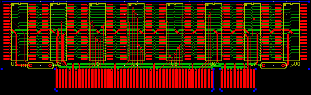
Another consideration of using edge connections as opposed to pins is if the pin header is on the motherboard (as it appears you are planning) then the mating receptacle has to be mounted to the memory module, which might complicate the physical construction. With edge connections, nothing has to be attached to the memory module PCB except the components. With a four-layer module, it should be possible to eliminate decoupling capacitors, since the power and ground planes act as the plates of a large capacitor.

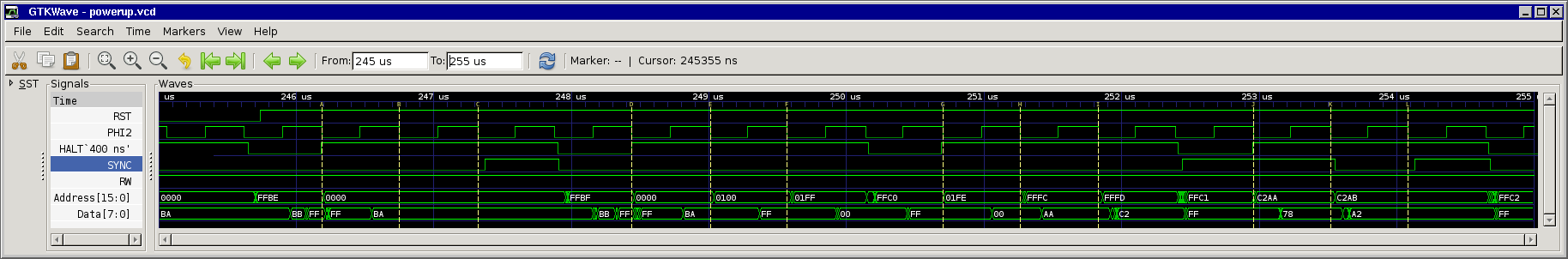
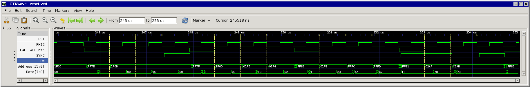
I recall the days when memory was sold as SIPs, which plugged into a receptacle on the motherboard. Aside from the ease at which the pins could be broken off a SIP, it was discovered that the receptacle introduced undesirable reactive effects. You don't see SIP memory modules anymore. I'm sure the industry would have stayed with them if it produced better (and less expensive) results. Either way, a receptacle of some kind will be required.

_________________
x86?  We ain't got no x86.  We don't NEED no stinking x86!


Top
 Profile  
Reply with quote  
 Post subject:
PostPosted: Wed Oct 13, 2010 11:36 pm 
Offline

Joined: Sat Jan 04, 2003 10:03 pm
Posts: 1706
Way off topic, but I can foresee a future where proximity connections are the wave of the future. Cheaper (no connectors) and potentially just as fast (near-field B-field communications emit much less RF than anything resembling radio antennas, which means you don't need as much shielding and no FCC license), the only hard requirement would be your components remaining within some finite distance of each other.

BDD and Garth, what I love about your arguments is that you have two experienced digital electronics engineers duking it out on the intellectual battlefield of experience, and everyone else in the galleries just sucks up bits of crumpled experience here and there, hopefully synthesizing a bigger, more complete synthesis of information useful for future projects. I know *I* am benefiting from this.


Top
 Profile  
Reply with quote  
 Post subject:
PostPosted: Thu Oct 14, 2010 12:11 am 
Offline
User avatar

Joined: Thu May 28, 2009 9:46 pm
Posts: 8176
Location: Midwestern USA
kc5tja wrote:
BDD and Garth, what I love about your arguments is that you have two experienced digital electronics engineers duking it out on the intellectual battlefield of experience...

Now if I could only figure out how to change that burned out light bulb in the garage... :)

As for the "duking it out" part, it's a war in which the opposing forces run around pointing sawed-off broom handles at each other and yelling "Bang! Bang!" When they're worn out from running and yelling they all go to the local tavern and swill beer together. :twisted:

_________________
x86?  We ain't got no x86.  We don't NEED no stinking x86!


Top
 Profile  
Reply with quote  
 Post subject:
PostPosted: Thu Oct 14, 2010 1:47 am 
Offline
User avatar

Joined: Thu Mar 11, 2004 7:42 am
Posts: 362
GARTHWILSON wrote:
I'm sure I saw writes (ie, R/W\ was low) but I'd have to dig it up to be more than 90% sure. The WDC manual also says they are writes, with R/W\ low.


Based on the quick experiments I ran way back when, the 65C02 wrote but the NMOS 6502 didn't. From the old thread here:

viewtopic.php?p=2959#2959


Top
 Profile  
Reply with quote  
Display posts from previous:  Sort by  
Post new topic Reply to topic  [ 86 posts ]  Go to page Previous  1, 2, 3, 4, 5, 6  Next

All times are UTC


Who is online

Users browsing this forum: No registered users and 6 guests


You cannot post new topics in this forum
You cannot reply to topics in this forum
You cannot edit your posts in this forum
You cannot delete your posts in this forum
You cannot post attachments in this forum

Search for:
Jump to: