Are you confident there's no need for diodes to prevent back-feed? Upthread, I came close to getting tripped up on that point.
I don't believe so. [...] If [the 4067 is] selected - and only one will be selected at once - it will decode the 1-of-16 row in its block, and it will be pulled to ground. But other pins on the same chip remain high impedance
Expressed
verbally, that line of reasoning seems pretty solid. But IME this stuff is
awfully slippery to think about!

And -- as was the case with my own circuit upthread -- expressing the thing as a
diagram yields a different and gloomier conclusion.

In the image below, I've made some connections which plausibly might arise in real life. Drawn in purple is a line driven by Address 6, and when it goes low it pulls low the input nibl2, as desired. But that low signal will also propagate in an
undesired way, backwards along the connections drawn in green (which are only supposed to go low for Address 2). Unless I'm somehow missing something, diodes or some other measure *are* required to prevent the back-feed.
Or, a rather different approach. Can the desired connections be manually established with just a dab of solder? You'd need a clever pattern [...]
I think you could easily define such a footprint, but you would need to be careful about defining the solder resist...
Yes, it's this business about managing the solder resist which is outside my ken. I'm sure the desired deviousness is
possible 
but what I don't know is how well it's supported by the various CAD programs and the various PCB fabs. (Ditto for my questions about vias in four-layer boards.)
FWIW, here (below) is my first pass on (just for example) a SP8T switch.
Either...
- - a dab of solder would manually be placed in such a way as to connect one of the two center terminals to one of the eight surrounding pads, or...
- that same connection would be ready-made as a slender copper trace, removable if so desired by use of a Dremel or X-acto knife.
Of course the opposite side of the board has eight traces running vertically (attaching to the vias, which I've drawn as yellow donuts).
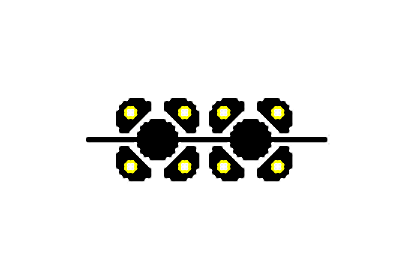
- SP8T switch (one).png (6.39 KiB) Viewed 980 times
The second image shows a space-efficient way of packing multiple switches together. As you can see, they're compressed in the vertical dimension because each row of pads serves both the switch above and the switch below.
It goes without saying that there will be a LOT of vias. And IIRC, Express PCB charges extra for that sort of thing. Is this common? Will via cost be an issue?
-- Jeff
ps- I think the density could be doubled by using a four-layer board with switches on both sides.
