6502.org Forum  Projects  Code  Documents  Tools  Forum
It is currently Mon May 13, 2024 2:03 am

All times are UTC


Post new topic Reply to topic  [ 45 posts ]  Go to page 1, 2, 3  Next
Author Message
PostPosted: Tue Jul 05, 2022 6:30 pm 
Offline
User avatar

Joined: Fri Dec 12, 2008 10:40 pm
Posts: 1001
Location: Canada
In support of my arguments over on this thread: http://forum.6502.org/viewtopic.php?f=4&t=6594

I'm going to do a few real-life experiments. This first one is to see the drive capability of a 74LSxx chip in various environments. I'll check it out in a typical situation where it's original designers expected it to live .. driving 6 full TTL loads. The test load is a 7404. Next I'll check out how well we can drive a load more in tune with our projects .. 6 CMOS loads (a 74HC04). The finally I will overload it beyond the worst case specifications (6 full TTL loads + 8.2K resistor) and see how it does.

Here is it driving the 6 full TTL loads. Measured current draw at the high level is 114uA.
Attachment:
6ttl.jpg
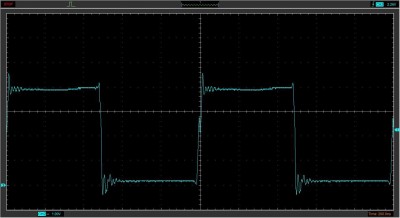
6ttl.jpg [ 78.7 KiB | Viewed 910 times ]
We can see, as expected it fully meets and nicely exceeds specifications for both TTL and CMOS environments.


Now let's have a look at it driving the 6 CMOS loads. Measured current at the high level is 0.58uA. This is basically an open circuit form the perspective of the 74LS chip.
Attachment:
6cmos.jpg
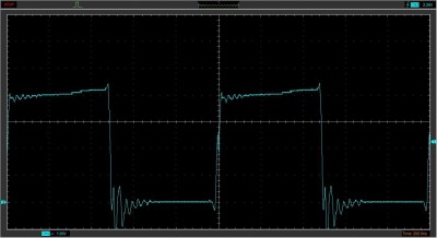
6cmos.jpg [ 80.05 KiB | Viewed 910 times ]
The lack of any reasonable load has this ringing a little, but the 74LS output has absolutely no problem exceeding CMOS input specifications. This is basically no-load performance of the chip. I suspect it would have no issue driving 50 worse case CMOS loads, excepting faulty chips.

Now let's over-load the thing. 6 full TTL loads plus a 8K2 resistor. Measured current is 532uA. This would amount to 13 worst case full TTL loads or about 5,000 typical CMOS loads (ignoring capacitance). Most of us would not exceed that (I think).
Attachment:
6ttl8k2.jpg
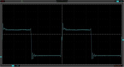
6ttl8k2.jpg [ 79.38 KiB | Viewed 910 times ]
Even under these conditions it betters typical CMOS requirements and beats the usual worst case (.7Vcc). It certainly far exceeds "worst case" TTL requirements.

Next I'll test some typical RAM, ROM and PLD devices to see if we should wonder too much why they actually work when the out dated spec sheet test conditions say they might, rarely if ever, not work.

_________________
Bill


Top
 Profile  
Reply with quote  
PostPosted: Tue Jul 05, 2022 6:42 pm 
Offline
User avatar

Joined: Fri Aug 30, 2002 1:09 am
Posts: 8433
Location: Southern California
It looks like the rise time is about 30ns, about twice as long as the fall time. Is that what you get when you expand it out to get that timing resolution? Does the 'scope probe add 20pF? 10pF? Something else?

_________________
http://WilsonMinesCo.com/ lots of 6502 resources
The "second front page" is http://wilsonminesco.com/links.html .
What's an additional VIA among friends, anyhow?


Top
 Profile  
Reply with quote  
PostPosted: Tue Jul 05, 2022 7:12 pm 
Offline
User avatar

Joined: Fri Dec 12, 2008 10:40 pm
Posts: 1001
Location: Canada
Because the rise and fall times were fairly consistent across the 3 loads it did not raise a red flag. I was just looking to see if the VIl and VIh specs were being met for the different environments. I will measure the scope lead capacitance and the rise/fall times.

Okay, got the timing and cable measurements:

6 CMOS loads - rise = 39ns, fall = 24ns

6 TTL loads - rise = 41ns, fall = 26ns

Overload - rise = 36.5 ns, fall =27.5ns

Scope probe and lead (attached to scope) measures 17pF

_________________
Bill


Top
 Profile  
Reply with quote  
PostPosted: Tue Jul 05, 2022 7:24 pm 
Offline

Joined: Fri Dec 21, 2018 1:05 am
Posts: 1076
Location: Albuquerque NM USA
I know TI published logic family's typical characteristic in their data book. I looked up chapter 1 of my TTL,LS,S databook and see many detailed charts of output characteristics vs temperature and load. Voh of 3.4V at room temperature, no load is typical. I know there are similar typical characteristic graphs for TI's HC, HCT, AC ACT family. I know I had these books but they are probably moth-eaten in back of my garage!
Bill


Top
 Profile  
Reply with quote  
PostPosted: Tue Jul 05, 2022 7:31 pm 
Offline
User avatar

Joined: Fri Aug 30, 2002 1:09 am
Posts: 8433
Location: Southern California
Make sure you measure the rise time to the CMOS threshold with the CMOS load, and the TTL threshold with the TTL load, which I think will make the CMOS load appear to take longer since the voltage has to come up higher which will take more time. A rise time of 25-30ns won't be nearly fast enough though in situations where we're trying to run a 65xx at 20MHz and a clock period is 50ns and the φ2-high or -low time is only 25ns. In that case, a lot more drive strength will be needed to charge up the bus capacitance in just a few ns.

_________________
http://WilsonMinesCo.com/ lots of 6502 resources
The "second front page" is http://wilsonminesco.com/links.html .
What's an additional VIA among friends, anyhow?


Top
 Profile  
Reply with quote  
PostPosted: Tue Jul 05, 2022 7:32 pm 
Offline
User avatar

Joined: Fri Dec 12, 2008 10:40 pm
Posts: 1001
Location: Canada
plasmo wrote:
Voh of 3.4V at room temperature, no load is typical.
Bill
This sounds very low in my experience. The TI sheet I have for their 74LSXX quotes 3.4V @ 400uA for the typical value. My guess is that their is a fudge (CYA) factor in there as I'm getting 3.6V @ a 25% overload. Exact same result for 3 different chips.

_________________
Bill


Top
 Profile  
Reply with quote  
PostPosted: Tue Jul 05, 2022 7:41 pm 
Offline
User avatar

Joined: Fri Dec 12, 2008 10:40 pm
Posts: 1001
Location: Canada
GARTHWILSON wrote:
A rise time of 25-30ns won't be nearly fast enough though in situations where we're trying to run a 65xx at 20MHz and a clock period is 50ns and the φ2-high or -low time is only 25ns. In that case, a lot more drive strength will be needed to charge up the bus capacitance in just a few ns.[/color]


Agreed. I think, however, we will see much improved rise and fall times from the CMOS devices in the next stage of the test.

This one was entirely focused on loading. 74LSXX would not be expected to perform well at very high frequencies. However, they should perform well enough at frequencies under about 8MHz. All that said, I would not use TTL at all these days at anything above 2MHz.

BTW, does anyone know why slew rates are not a part of the spec sheets for these TTL parts?

_________________
Bill


Top
 Profile  
Reply with quote  
PostPosted: Tue Jul 05, 2022 7:46 pm 
Offline

Joined: Sat Feb 19, 2022 10:14 pm
Posts: 147
Very informative. Thanks for posting!


Top
 Profile  
Reply with quote  
PostPosted: Tue Jul 05, 2022 10:26 pm 
Offline
User avatar

Joined: Sun Jun 30, 2013 10:26 pm
Posts: 1929
Location: Sacramento, CA, USA
That little dip in the middle of the positive edge on all three traces ... that's not ringing is it? It looks to me like it's in a very bad place if we're worried about glitches, but I'll defer to the more experienced folks to confirm or deny this.

_________________
Got a kilobyte lying fallow in your 65xx's memory map? Sprinkle some VTL02C on it and see how it grows on you!

Mike B. (about me) (learning how to github)


Top
 Profile  
Reply with quote  
PostPosted: Tue Jul 05, 2022 10:40 pm 
Offline
User avatar

Joined: Fri Dec 12, 2008 10:40 pm
Posts: 1001
Location: Canada
I think it's a bypassing/inductance issue. This was just a first pass at all this and was quickly thrown together on a solderless breadboard. I'll do a little sleuthing to figure it out and see if I can clean up things before I move ahead.

_________________
Bill


Top
 Profile  
Reply with quote  
PostPosted: Tue Jul 05, 2022 11:38 pm 
Offline
User avatar

Joined: Thu May 28, 2009 9:46 pm
Posts: 8182
Location: Midwestern USA
BillO wrote:
plasmo wrote:
Voh of 3.4V at room temperature, no load is typical.
Bill
This sounds very low in my experience. The TI sheet I have for their 74LSXX quotes 3.4V @ 400uA for the typical value. My guess is that their is a fudge (CYA) factor in there as I'm getting 3.6V @ a 25% overload. Exact same result for 3 different chips.

3.4 volts is based upon the two diode drops when the totem-pole output is driving high. There is also internal resistance in there. 3.4 volts is theoretical. Temperature and other factors will conspire to limit VOH to something less.

_________________
x86?  We ain't got no x86.  We don't NEED no stinking x86!


Top
 Profile  
Reply with quote  
PostPosted: Wed Jul 06, 2022 5:41 am 
Offline
User avatar

Joined: Thu Dec 11, 2008 1:28 pm
Posts: 10800
Location: England
barrym95838 wrote:
That little dip in the middle of the positive edge on all three traces ... that's not ringing is it? It looks to me like it's in a very bad place ...


BillO wrote:
I think it's a bypassing/inductance issue. This was just a first pass at all this and was quickly thrown together on a solderless breadboard. I'll do a little sleuthing to figure it out and see if I can clean up things before I move ahead.


I might guess it's ground bounce (very much related) - worth mentioning, I think, because every chip, and the scope probe, will reference a signal level to their local ground. The scope probe, particularly, needs to be seeing something very like the same ground as the chip that's receiving the signal:
BigEd wrote:
.Make sure you've adjusted your probes correctly ("compensated" or "calibrated" them) and consider using the twirly spring tactic for grounding the probe.
https://electronics.stackexchange.com/q ... und-spring.


Top
 Profile  
Reply with quote  
PostPosted: Fri Jul 08, 2022 10:29 pm 
Offline
User avatar

Joined: Fri Dec 12, 2008 10:40 pm
Posts: 1001
Location: Canada
I re-built the initial test circuit on a PCB keeping the connections as short as possible and there has been improvement. The power rails are .1" wide traces of 1oz copper and bypass capacitors have been placed between the power pins of each IC and between the ICs.

The total capacitance of the 6 CMOS inputs measured in circuit is 4.6pF (Edit: This was a measurement error. The actual value is 36.4 pF of which 11.6 is contributed by the circuit). Add to that the scope/probe capacitance which measures 16pF without the clip.

Rise and fall times have improved dramatically. Rise (to 3.5V)is now 15ns and fall is 5ns.

Now, using a whisker ground on the probe most of the ringing is gone, especially on the falling edge. However, the dip in the middle of the rising edge is still there. It's far less, but still there. It also reduces as the load increases. Both 74xx and 74lsxx produce that dip. 74ACxx does not.

Is it a measurement artifact?

_________________
Bill


Last edited by BillO on Sun Jul 10, 2022 5:24 pm, edited 1 time in total.

Top
 Profile  
Reply with quote  
PostPosted: Fri Jul 08, 2022 10:38 pm 
Offline
User avatar

Joined: Fri Aug 30, 2002 1:09 am
Posts: 8433
Location: Southern California
BillO wrote:
The total capacitance of the 6 CMOS inputs measured in circuit is 4.6pF. Add to that the scope/probe capacitance which measures 16pF without the clip.

"Total," as in the whole set together was only 4.6pF, rather than all inputs averaged 4.6pF each? That's good news, as the data sheets usually say 5pF max per input.

Quote:
However, the dip in the middle of the rising edge is still there. It's far less, but still there. It also reduces as the load increases. Both 74xx and 74lsxx produce that dip. 74ACxx does not.

Is it a measurement artifact?

If it's not from groundbounce, I wonder if it's some sort of crossover distortion in the IC itself.

_________________
http://WilsonMinesCo.com/ lots of 6502 resources
The "second front page" is http://wilsonminesco.com/links.html .
What's an additional VIA among friends, anyhow?


Top
 Profile  
Reply with quote  
PostPosted: Fri Jul 08, 2022 10:47 pm 
Offline
User avatar

Joined: Fri Dec 12, 2008 10:40 pm
Posts: 1001
Location: Canada
GARTHWILSON wrote:
"Total," as in the whole set together was only 4.6pF, rather than all inputs averaged 4.6pF each? That's good news, as the data sheets usually say 5pF max per input.
Yes, that's the total of all 6 CMOS inputs as a group.

I should pull the chip to see how much of that is the circuit.

Edit: Made an little error. Yeah, that 4.6 pF was just a single input. All 6 in circuit measure 36.4 pF of which 11.6 is contributed by the circuit. So the 6 inputs total 24.8 pF (or an average of 4.1) which is more in-line with specs.

Quote:
If it's not from groundbounce, I wonder if it's some sort of crossover distortion in the IC itself.


I guess it could be. That would be a red flag against using TTL to drive CMOS.

_________________
Bill


Last edited by BillO on Fri Jul 08, 2022 11:10 pm, edited 1 time in total.

Top
 Profile  
Reply with quote  
Display posts from previous:  Sort by  
Post new topic Reply to topic  [ 45 posts ]  Go to page 1, 2, 3  Next

All times are UTC


Who is online

Users browsing this forum: No registered users and 11 guests


You cannot post new topics in this forum
You cannot reply to topics in this forum
You cannot edit your posts in this forum
You cannot delete your posts in this forum
You cannot post attachments in this forum

Search for:
Jump to: