6502.org Forum  Projects  Code  Documents  Tools  Forum
It is currently Sat May 18, 2024 7:31 pm

All times are UTC


Post new topic Reply to topic  [ 65 posts ]  Go to page Previous  1, 2, 3, 4, 5  Next
Author Message
PostPosted: Mon Jan 10, 2022 5:29 pm 
Offline
User avatar

Joined: Fri Jun 22, 2012 7:39 am
Posts: 201
> It looks like the inverter for brk6_latch1 is missing.

Ah, I get it, as a result of the optimization everything is fine there, sorry :)


Attachments:
brk6_demorgan.jpg
brk6_demorgan.jpg [ 94.29 KiB | Viewed 644 times ]

_________________
6502 addict
Top
 Profile  
Reply with quote  
PostPosted: Tue Jan 11, 2022 8:54 am 
Offline
User avatar

Joined: Fri Nov 09, 2012 5:54 pm
Posts: 1394
org, nice going. :)


To the readers of this thread:
The situation is, that we have two teams which had used different approaches, notations and logic symbols for dissecting a CPU core.
//Assuming that the 6502 core and the 6509 core are identical at logic design level.
So it is fully normal to have false positives when cross_checking the results of both teams for errors.

For instance, I'm an old school hardware guy with absolutely no LogiSim experience,
and to me it wasn't obvious that a transparent latch like 74373 could have an inverted and a non_inverted output,
what had confused me a bit, sorry. :)

Also, in my schematics the disabling of the PLA product terms 92:T2.ANY_ABS, 99:T3.ANY_ABS, 145:Tx.IMPL
happens inside the PLA, while the 'org' schematics had moved that part into the random logic area,
what had confused me a bit, too.

So please see them false positives as a proof that we are just trying to do a good job while cross_checking the results. :)


Top
 Profile  
Reply with quote  
PostPosted: Thu Jan 13, 2022 7:55 pm 
Offline
User avatar

Joined: Fri Jun 22, 2012 7:39 am
Posts: 201
I did a little work on the Data Path diagram at the bottom.

- Missing S and ADL connection (S/ADL)
- The fact of loading direct and inverse value to the BI ALU latch is not reflected (DB/ADD, NDB/ADD)
- Zero load command is not displayed on the AI latch (0/ADD)
- ADL/ADD connects ADL and BI (not AI)
- Current value refresh commands are not displayed (S/S, PCL/PCL, PCH/PCH)
- Instead of "BCD-detect" made ADD (Adder Hold) and output to ADL and SB buses from it
- A -> AC (not to be confused with A Input)


Attachments:
datapath.png
datapath.png [ 31.77 KiB | Viewed 598 times ]

_________________
6502 addict
Top
 Profile  
Reply with quote  
PostPosted: Fri Jan 14, 2022 10:14 am 
Offline
User avatar

Joined: Fri Jun 22, 2012 7:39 am
Posts: 201
In addition to the previous post.

- CGH and CGL are mixed up
- Adding a cleaner version of the diagram


Attachments:
datapath2.png
datapath2.png [ 26.49 KiB | Viewed 571 times ]

_________________
6502 addict
Top
 Profile  
Reply with quote  
PostPosted: Fri Jan 14, 2022 12:03 pm 
Offline
User avatar

Joined: Fri Nov 09, 2012 5:54 pm
Posts: 1394
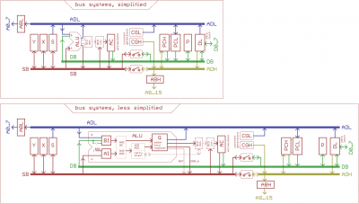
I admit that I was in a hurry when drawing the block diagram with the bus systems,
it was the last step of the dissection.

It isn't exactly a data path diagram, because it shows the data path plus the address path. :)
Block diagram intentionally was kept as simply as possible to give an overview.
Don't worry, I'm adding a more detailed version.

Quote:
- Missing S and ADL connection (S/ADL)

My mistake, fixed.

Quote:
- The fact of loading direct and inverse value to the BI ALU latch is not reflected (DB/ADD, NDB/ADD)
- Zero load command is not displayed on the AI latch (0/ADD)

I consider the AI and BI latches (plus the related circuitry) to be integral part of the ALU.

Quote:
- ADL/ADD connects ADL and BI (not AI)

My mistake, fixed.

Quote:
- Current value refresh commands are not displayed (S/S, PCL/PCL, PCH/PCH)

I consider the refresh paths to be integral part of the registers.

Quote:
- Instead of "BCD-detect" made ADD (Adder Hold) and output to ADL and SB buses from it

I consider the 'adder hold register' to be integral part of the ALU.


Quote:
- A -> AC (not to be confused with A Input)

In Hanson's block diagram, the accumulator is labeled 'AC', so I'm changing 'A' to 'AC'.

Quote:
- CGH and CGL are mixed up

Dang. How could this happen ? :)
My mistake, fixed.

Attachment:
6509_core_bus.png
6509_core_bus.png [ 71.03 KiB | Viewed 565 times ]


Top
 Profile  
Reply with quote  
PostPosted: Mon Jan 31, 2022 8:01 am 
Offline
User avatar

Joined: Fri Jun 22, 2012 7:39 am
Posts: 201
Small case SB_S:

For some reason, the 6-nor is split into two gates (in the demorganized version 4or + 2or).

I am attaching the transistor circuit and a piece of dissection to get the #SB/S.


Attachments:
SB_S_6nor.jpg
SB_S_6nor.jpg [ 19.71 KiB | Viewed 518 times ]
SB_S.jpg
SB_S.jpg [ 90.06 KiB | Viewed 518 times ]

_________________
6502 addict
Top
 Profile  
Reply with quote  
PostPosted: Mon Jan 31, 2022 8:16 am 
Offline
User avatar

Joined: Fri Jun 22, 2012 7:39 am
Posts: 201
Case SBXY:

On the transistor circuit, the SBXY intermediate signal (SB>X,Y) comes in only one place - ZTST.


Attachments:
SBXY.jpg
SBXY.jpg [ 286.88 KiB | Viewed 517 times ]

_________________
6502 addict
Top
 Profile  
Reply with quote  
PostPosted: Mon Jan 31, 2022 11:07 am 
Offline
User avatar

Joined: Fri Nov 09, 2012 5:54 pm
Posts: 1394
org wrote:
Small case SB_S:

For some reason, the 6-nor is split into two gates (in the demorganized version 4or + 2or).

Reason was, that there were no 6or or 8or logic gates in the libraries of the CAD software I'm using.

org wrote:
Case SBXY:

On the transistor circuit, the SBXY intermediate signal (SB>X,Y) comes in only one place - ZTST.

Ah, that... maybe I had skipped a step during optimisation:

Attachment:
sb_db.png
sb_db.png [ 84.51 KiB | Viewed 507 times ]

0)
org:ZTST = SB>A | AND,BIT | SB>X,Y | org:T6
the output of an AND gate goes into the "SB<>DB# NOR": NOT(AND,BIT) & org:ZTST

1)
so we could consider that input of the "SB<>DB# NOR" fed by the AND
to be the equivalent of the output of a three input OR gate:
SB>A | SB>X,Y | org:T6

2)
So I had pushed that three input OR gate into the "SB<>DB# NOR gate". :)


Top
 Profile  
Reply with quote  
PostPosted: Tue Feb 01, 2022 5:40 pm 
Offline
User avatar

Joined: Fri Jun 22, 2012 7:39 am
Posts: 201
Cosmetic case DSA#:

I noticed that DSA# is obtained in random logic, but is not mentioned in the command block.
We know where it comes from, but for example, who will study it, will not immediately notice it.


Attachments:
DSA_2.jpg
DSA_2.jpg [ 84.23 KiB | Viewed 486 times ]
DSA.jpg
DSA.jpg [ 42.63 KiB | Viewed 486 times ]

_________________
6502 addict
Top
 Profile  
Reply with quote  
PostPosted: Wed Feb 02, 2022 7:58 am 
Offline
User avatar

Joined: Fri Nov 09, 2012 5:54 pm
Posts: 1394
Good point,
so I added 6 signals to that part of my schematic:

0>ADL0, 0>ADL1, 0>ADL2,
DSA#, 0>ADH8, AVR.

Attachment:
dsa.png
dsa.png [ 28.54 KiB | Viewed 472 times ]


BTW: could you please label the output signals of "Pattern Readout" and "V. Inversion"
in the silicon pictures of the NES PPU ? :)


Top
 Profile  
Reply with quote  
PostPosted: Wed Feb 02, 2022 9:35 am 
Offline
User avatar

Joined: Fri Jun 22, 2012 7:39 am
Posts: 201
ttlworks wrote:
BTW: could you please label the output signals of "Pattern Readout" and "V. Inversion"
in the silicon pictures of the NES PPU ? :)


Done :) If there is anything else, you can safely go through the Issues section: https://github.com/emu-russia/breaks/issues

_________________
6502 addict


Top
 Profile  
Reply with quote  
PostPosted: Wed Feb 02, 2022 12:41 pm 
Offline
User avatar

Joined: Fri Nov 09, 2012 5:54 pm
Posts: 1394
Thanks. :)


Top
 Profile  
Reply with quote  
PostPosted: Fri Feb 04, 2022 3:50 pm 
Offline
User avatar

Joined: Fri Jun 22, 2012 7:39 am
Posts: 201
Case BCD_Carry:

To calculate DC3, AND0 and OR0 are mixed up.

I even did a unit test to see if there was an error.

This is the last circuit that completes the series of checks between your circuits and ours. I can say that our schematics had a lot more errors and this comparison helped us a lot. Great work, thank you!


Attachments:
nand0_nor0_tran.jpg
nand0_nor0_tran.jpg [ 17.57 KiB | Viewed 431 times ]
ttlworks_bcd_carry.jpg
ttlworks_bcd_carry.jpg [ 203.89 KiB | Viewed 431 times ]

_________________
6502 addict
Top
 Profile  
Reply with quote  
PostPosted: Mon Feb 07, 2022 10:03 am 
Offline
User avatar

Joined: Fri Nov 09, 2012 5:54 pm
Posts: 1394
org wrote:
Case BCD_Carry:

To calculate DC3, AND0 and OR0 are mixed up.

Woot: eventually a nice electrical error in my schematics. :)
Error confirmed and fixed, thanks.

There are two possible ways of implementing a carry chain,
and it looks like I had mixed something up by accident.

Attachment:
6509_carry.png
6509_carry.png [ 49.15 KiB | Viewed 408 times ]


;---

Also, in my schematics the ALU input carry sometimes was labeled 'ALU_cin#' instead of 'Ci0#'.
Fixed that to make things more consistent.

;---

org wrote:
This is the last circuit that completes the series of checks between your circuits and ours. I can say that our schematics had a lot more errors and this comparison helped us a lot. Great work, thank you!

Thanks for the appreciation and the kind words.
You and your team also did a great work with that 6502 dissection:
not many people out there would have been able to do something like this.
6502 core is a very compact, very tricky beast.

This comparison has helped the whole community a lot:
We now have schematics of the 6502 core in optimized (demorganzied) form and in not_optimized form,
also we were able to identify all of the functional blocks within the control circuitry.
It should be possible now for the community to figure out, what exactly happens inside a 6502 core, and why.


Top
 Profile  
Reply with quote  
PostPosted: Tue Feb 15, 2022 10:00 am 
Offline
User avatar

Joined: Fri Nov 09, 2012 5:54 pm
Posts: 1394
For supporting "breaking NES book, 6502 core",
I'm posting my big 6509 schematic broken into smaller pieces,
with signal and flipflop names changed according to that book.

Attachment:
nes_book.zip [1.71 MiB]
Downloaded 37 times

Дава́й. :)


Top
 Profile  
Reply with quote  
Display posts from previous:  Sort by  
Post new topic Reply to topic  [ 65 posts ]  Go to page Previous  1, 2, 3, 4, 5  Next

All times are UTC


Who is online

Users browsing this forum: JohanFr and 4 guests


You cannot post new topics in this forum
You cannot reply to topics in this forum
You cannot edit your posts in this forum
You cannot delete your posts in this forum
You cannot post attachments in this forum

Search for:
Jump to: