6502.org Forum  Projects  Code  Documents  Tools  Forum
It is currently Sat Apr 27, 2024 5:02 pm

All times are UTC


Post new topic Reply to topic  [ 558 posts ]  Go to page Previous  1, 2, 3, 4, 5 ... 38  Next
Author Message
 Post subject: Re: TTL 6502 Here I come
PostPosted: Sun Oct 25, 2015 9:25 am 
Offline
User avatar

Joined: Thu Dec 11, 2008 1:28 pm
Posts: 10793
Location: England
Quite right about the open drain MOSFETS Drass - they are the conditional pulldowns which operate on a precharged bus to construct constants such as 0, 1, fe and so on.

One trick in the 6502 is the use in some places of phi2/phi1 cycles instead of phi1/phi2 cycles: you'll see for example many datapath control signals are valid over phi2/phi1, which means they can safely control the datapath activities which occur over phi1/phi2. I think...

You mention A INPUT, B INPUT as registers, Drass, and I see that Hanson labels them as such (these are the busses named as alua and alub in visual6502, the byte-wide collections of signals which form the inputs to the ALU)... but I'm not sure whether or not to think of them that way. I think I must, although there's no recirculation so they are latches rather than flops. They are clocked by datapath control signals - a case of gated clocks - not by the chip-wide clocks. Looking closer, I see the ALU output is also a latch, this time clocked unconditionally. Whereas the accumulator does recirculate, but is loaded conditionally by SBAC used as a clock. The merging of a clock and a multiplexor is one of the efficiencies in 6502 which keeps the transistor count so low.

I'm sure you're right though that splitting ALU action over two cycles - operate and then writeback - helped keep down the path length and bus complexity in the 6502.

(I'll second Arlet's recommendation to study his core!)


Top
 Profile  
Reply with quote  
 Post subject: Re: TTL 6502 Here I come
PostPosted: Sun Oct 25, 2015 6:05 pm 
Offline
User avatar

Joined: Thu Dec 11, 2008 1:28 pm
Posts: 10793
Location: England
BigEd wrote:
Now, I think there might be a 4000 chip which offers quad (or possibly octal) bidirectional connectivity.

Aha - it's the 4066.
Image
(Thanks to Gerrit Heitsch on cbm-hackers who just happened to post this info today!)


Top
 Profile  
Reply with quote  
 Post subject: Re: TTL 6502 Here I come
PostPosted: Mon Oct 26, 2015 5:12 am 
Offline
User avatar

Joined: Sun Oct 18, 2015 11:02 pm
Posts: 428
Location: Toronto, ON
Arlet wrote:
If you know verilog, you could also take a look at my 6502 verilog core, which gets to the exact same amount of cycles, but in a different way (there are no internal buses for instance)

https://github.com/Arlet/verilog-6502


Thanks for the pointer Arlet. I don't know Verilog, but I will read up a bit and dig in. I'm very interested to see what you've done. (Any pointers to a good Verilog intro online?)

I took a look at the propagation delay through the data path and it appears I've been unduly harsh on my design. It turns out that moving data around the busses is not nearly as expensive as I thought. The combinatorial logic in decoders and adders is far more costly. As an example, it takes 180ns to go from clock tick to the control signals being output, but only 120ns to put an address on the bus (using 74HC logic). By far the most expensive operation is incrementing the program counter (250ns) and I can think of a couple of ways of optimizing that without complicating the microcode.

By a rough estimate, I expect the processor will run at least at 2MHz as is and that already exceeds my original goal of matching the 1MHz of the C64. So, I'm reasonably happy with the tradeoff of simplicity vs. speed at this point. That said, I'm eager to learn what I can from studying the visual 6502 traces and Arlet's core. There is no question the 6502 is pulling off some interesting magic and I want to understand that better.

Cheers for now.

_________________
C74-6502 Website: https://c74project.com


Top
 Profile  
Reply with quote  
 Post subject: Re: TTL 6502 Here I come
PostPosted: Mon Oct 26, 2015 5:31 am 
Offline
User avatar

Joined: Sun Oct 18, 2015 11:02 pm
Posts: 428
Location: Toronto, ON
BigEd wrote:
One trick in the 6502 is the use in some places of phi2/phi1 cycles instead of phi1/phi2 cycles: you'll see for example many datapath control signals are valid over phi2/phi1, which means they can safely control the datapath activities which occur over phi1/phi2. I think...


Yes, I can see the signals acting over both phi1/2 and phi2/1. For sure there is control over independent processes occurring over both periods. Certainly there are things moving around every half cycle. It's tricky and clever.

Quote:
I'm sure you're right though that splitting ALU action over two cycles - operate and then writeback - helped keep down the path length and bus complexity in the 6502


Yes, I think so. Certainly the traces show clearly how the logic allows time for the ALU to operate and latch the result in the output register. And if in fact the inputs are being latched in the previous cycle, there is savings there too. I really need some solid time to "crack the code" on this. Sadly, I'll have to wait until next weekend for another few hours of uninterrupted study time.

_________________
C74-6502 Website: https://c74project.com


Top
 Profile  
Reply with quote  
 Post subject: Re: TTL 6502 Here I come
PostPosted: Mon Oct 26, 2015 9:39 am 
Offline
User avatar

Joined: Thu Dec 11, 2008 1:28 pm
Posts: 10793
Location: England
The 6502 detects PCL being FF with an 8-input gate (an 8-input NOR, because NMOS NOR is very much preferable to NMOS NAND for more than three inputs) and uses that as the carry into PCH. So there's just a little over 8 bits of ripple carry needed in a cycle.

I'm not aware than anyone has done any kind of timing analysis on the original 6502 - it would not be straightforward because it's not constructed purely from logic gates and flops. It's not too difficult to run a circuit level simulation but it's not quick!
viewtopic.php?p=13550#p13550
"it took about 30 mins to run through reset and then 20mins to do 10 cycles of instructions"


Top
 Profile  
Reply with quote  
 Post subject: Re: TTL 6502 Here I come
PostPosted: Mon Oct 26, 2015 2:22 pm 
Offline
User avatar

Joined: Fri Dec 11, 2009 3:50 pm
Posts: 3346
Location: Ontario, Canada
BigEd wrote:
BigEd wrote:
Now, I think there might be a 4000 chip which offers quad (or possibly octal) bidirectional connectivity.

Aha - it's the 4066.
Modern equivalents to the 4066 have much lower ON Resistance and faster enable/disable times -- and are available in octal configurations to boot! :mrgreen: Bidirectional connectivity is actually very well supported nowadays. As noted in this other post, the overall selection is startlingly extensive.

Here's some detail regarding a '245 bus "transceiver" implemented using MOSFET transmission gates similar to those in the 4066. Pin 1 -- which, on an ordinary '245, is the Direction input -- is a No-Connect. When enabled, the device behaves as a set of eight low-value resistors -- and resistors don't care about direction. :)

For typical applications the appeal of these products lies in their ability to connect two buses so data passes between them with virtually no propagation delay. But their similarity to 65xx internal logic makes them worth considering for your project.

cheers,
Jeff


Attachments:
alternative '245.gif
alternative '245.gif [ 10.21 KiB | Viewed 3352 times ]

_________________
In 1988 my 65C02 got six new registers and 44 new full-speed instructions!
https://laughtonelectronics.com/Arcana/ ... mmary.html


Last edited by Dr Jefyll on Mon Oct 26, 2015 2:32 pm, edited 2 times in total.
Top
 Profile  
Reply with quote  
 Post subject: Re: TTL 6502 Here I come
PostPosted: Mon Oct 26, 2015 2:29 pm 
Offline
User avatar

Joined: Sun Oct 18, 2015 11:02 pm
Posts: 428
Location: Toronto, ON
BigEd wrote:
The 6502 detects PCL being FF with an 8-input gate (an 8-input NOR, because NMOS NOR is very much preferable to NMOS NAND for more than three inputs) and uses that as the carry into PCH. So there's just a little over 8 bits of ripple carry needed in a cycle.


Exactly. A second NAND in series can also lookahead the carry for the final 4 bit adder. I think that's still cheaper than adder ripple.

There are other delays as well. Specifically, the INC circuit currently takes its input from the address bus because I also use it as an 8 bit circuit for SP and DPL and it's just convenient to do so. Given how often PC is incremented, however, it deserves it's own path. Tapping it's outputs directly will produce significant savings I think.

Quote:
I'm not aware than anyone has done any kind of timing analysis on the original 6502


Comparing a discrete logic microcode cpu to a PLA-sequenced NMOS microprocessor likely says very little about the relative merits of the design. Maching 1MHz is a rather arbitrary goal in that regard. That said, 6502 timing would be interesting of its own accord and I expect a lot could be learned from that. I don't know how the propagation delay of a given circuit varies between one etched in a chip and a discrete component. Let alone what impact other factors have, e.g. NMOS vs. CMOS, etc.

Quote:
the so-called precharge often fights against pulldowns during phi2 rseulting in an intermediate voltage

This is interesting. I thought of using pull-downs and pull ups on the bus to get free constants by tri-tasting everything on and letting the resistors set the bus value. Not sure how well that would work or how to analyze the associated delays.

_________________
C74-6502 Website: https://c74project.com


Top
 Profile  
Reply with quote  
 Post subject: Re: TTL 6502 Here I come
PostPosted: Mon Oct 26, 2015 2:49 pm 
Offline
User avatar

Joined: Sun Oct 18, 2015 11:02 pm
Posts: 428
Location: Toronto, ON
Dr Jefyll wrote:


For typical applications the appeal of these products lies in their ability to connect two buses so data passes between them with virtually no propagation delay. But their similarity to 65xx internal logic makes them worth considering for your project.

cheers,
Jeff


.25ns tpd. Wow. That is definitely worth incorporating! I'll spend some time looking at it. I suspect the impact will be very significant.

Thanks for suggesting it Jeff.

_________________
C74-6502 Website: https://c74project.com


Top
 Profile  
Reply with quote  
 Post subject: Re: TTL 6502 Here I come
PostPosted: Tue Oct 27, 2015 5:10 am 
Offline

Joined: Sun Apr 10, 2011 8:29 am
Posts: 597
Location: Norway/Japan
I purchased a small lot of those SN74*3245 chips (and also the 4245 variant), with a vague plan of incorporating them in a possible mixed 3.3V/5V design. I haven't used them yet, but the specifications and data sheets are interesting reads.

-Tor


Top
 Profile  
Reply with quote  
 Post subject: Re: TTL 6502 Here I come
PostPosted: Thu Oct 29, 2015 4:39 am 
Offline
User avatar

Joined: Sun Oct 18, 2015 11:02 pm
Posts: 428
Location: Toronto, ON
Unfortunately, some travel is preventing me from digging further into the 6502 internals at the moment. I did, however, get some time on a plane to look at the 74CBT3245 bus switch more closely and to examine the impact of other potential optimizations (e.g. increment circuit carry look-ahead). The result was pretty exciting as I think a significant savings in propagation delay is possible across the design. I ran some preliminary numbers and got the following cycle times (inclusive of decoding control ROM signals - in other words from clock tick to completed operation):

Memory read: 209ns
Increment Program Counter: 320ns
Register transfer (through ALU setting ZN flags): 285ns
ALU operation (setting Carry flag): 400ns

Incrementing the program counter is now not nearly the most expensive operation. Top honours now goes to the ALU, and more specifically, the overhead associated with resolving and storing the ripple carry to the final output. I will spend more time looking at this particular detail, but I am now much happier with the relative performance of these circuits. Most of the improvement can be credited to eliminating the delay imposed by buffers and muxes used to connect internal busses together (e.g., 74HC541 Octal Bus Buffer Enable Time = 32ns vs. the virtually instantaneous 74CBT3245). Thanks again Ed and Jeff for pointing me in this direction. Conservatively (by which I mean using the Maximum propagation delay figures for the HC logic family) the processor should run at 2.5MHz, which is a very satisfying figure (using "Typical" delays gets things up to almost 4MHz).

While speed is in itself not an objective for me, I am very happy to be able to incorporate these efficiencies without unduly complicating the circuits or the microcode. I would very much like this design to be easy to follow even for a relative newcomer to hardware design. I don't think any of these changes takes me further away from that goal.

I'm excited to share some schematics as things go along. With some luck, I will get some things done weekend and get something posted.

Cheers.

_________________
C74-6502 Website: https://c74project.com


Top
 Profile  
Reply with quote  
 Post subject: Re: TTL 6502 Here I come
PostPosted: Thu Oct 29, 2015 1:35 pm 
Offline
User avatar

Joined: Fri Dec 11, 2009 3:50 pm
Posts: 3346
Location: Ontario, Canada
Drass wrote:
e.g., 74HC541 Octal Bus Buffer Enable Time = 32ns vs. the virtually instantaneous 74CBT3245
I hope it's clear that FET bus switches drastically slash propagation delay only -- ie; not the enable/disable times. It still takes on the order of 10 ns (consult the datasheet) to turn the device on or off. That may be tolerable or not -- it depends on the application. But once the switch is turned on it behaves like a resistor (about 3 ohms in this case) which is pretty close to being just a piece of wire! Here's where the speed becomes impressive.

The usual notion of propagation delay (implying active internal circuitry) doesn't apply. But inevitably the bus being driven has some amount of capacitance to ground, and putting 3 ohms in series means it'll take longer to charge or discharge that capacitance. The delay is proportional to R*C, and the delay cited in the datasheet pertains to a 15 pF load IIRC -- which is probably less than the capacitance in your application, since you presumably have the inputs of several chips attached to each bus. (Each chip that's driven contributes 5 or 10 pF, as a ballpark figure.)

For this and other reasons you can't expect the propagation delay cited in the datasheet to apply in your application. But the FET switch's bidirectional nature makes it directly equivalent to what's under the hood of an actual 6502. Perhaps it's something that'll offer you some advantage. :)

-- Jeff

_________________
In 1988 my 65C02 got six new registers and 44 new full-speed instructions!
https://laughtonelectronics.com/Arcana/ ... mmary.html


Top
 Profile  
Reply with quote  
 Post subject: Re: TTL 6502 Here I come
PostPosted: Thu Oct 29, 2015 11:54 pm 
Offline
User avatar

Joined: Sun Oct 18, 2015 11:02 pm
Posts: 428
Location: Toronto, ON
Dr Jefyll wrote:
I hope it's clear that FET bus switches drastically slash propagation delay only -- ie; not the enable/disable times

Thanks for pointing this out Jeff. I had in fact missed it. For some reason, the Phillips data sheet I looked at listed only "tpd. ??? Anyway, as it turns out, the TI data sheet shows the enable time as 6ns at 5V, which is still more then fast enough for my purposes (hope I'm reading that correctly). Still very much worth incorporating into the design I think.

_________________
C74-6502 Website: https://c74project.com


Top
 Profile  
Reply with quote  
 Post subject: Re: TTL 6502 Here I come
PostPosted: Sat Oct 31, 2015 12:09 pm 
Offline
User avatar

Joined: Sun Oct 18, 2015 11:02 pm
Posts: 428
Location: Toronto, ON
I finally finished a schematic which I'm excited to share. Apologies in advance for the long post. I've tried to provide a thorough overview to try to make this as easy as possible to follow even for relative beginners like myself.

The schematic attached is for the CPU registers and associated logic. You might note the complete absence of 74CBT3245 ICs in the schematic. In the end, I felt I had not made very good use of these chips after all and decided instead to share the design as it was before, leaving in place unidirectional busses and the ICs I had selected previously. No doubt it will make sense to revisit this but I'll press on for now and learn as we go.

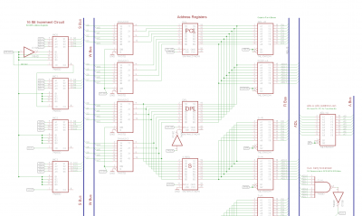
Looking at the schematic attached, the data path reflects the block diagram fairly closely and has the registers between the W Bus on the left and R Bus on the right. Each register is a 74HC574 with an “R” signal to output-enable them and a “WR” signal to clock them. To the right are the address registers (PCL/PCH, DPL/DPH, SP and T). Their outputs can be routed to the R Bus or to the the internal address bus “ADL/ADH”. Similarly, their inputs can come from the W Bus or the S Bus. The S Bus is the output of the INC16 circuit. See below.
Attachment:
Address Registers.png
Address Registers.png [ 148.53 KiB | Viewed 3208 times ]

On the far right are a pair of Carry Look Ahead NAND gates which feed the four 74HC283 INC16 adders. Addresses move from ADL/ADH to the external Address bus (“A Bus”) via /BE controlled 74HC541 buffers. In addition, the /ADHS.A signal sets the high-byte of the address to either ADH or a fixed value of $00, $01 or $FF depending on the address mode (ZDP, SP, FDP respectively).

DPH can be loaded directly from the external Data Bus by “DPH.LD” but it's not connected to the S Bus. Incrementing DP in fact only increments the lower 8 bits in DPL. The consequence is that DP will “warp-around” the same page if a page boundary is crossed when resolving the high-byte of an indirect address. This is also the NMOS 6502 behaviour.

IR is also loaded in parallel from the Data Bus during Fetch-Opcode operations ("IR.LD" selects that), or from the W Bus during interrupt processing. IR outputs directly to the Opcode lines (OP0 - OP7) which in turn feed the Control ROMs. The “INT” control signal is high during the first cycle of interrupt processing and thereby forces the Opcode to zero through the OP.LOGIC0 buffer.

The final item on the data path is the “R->DB" 74HC541 buffer which connects the R Bus to the external Data Bus for memory write operations. /MEM.W and /BE signals together enable this buffer for the full write-cycle.

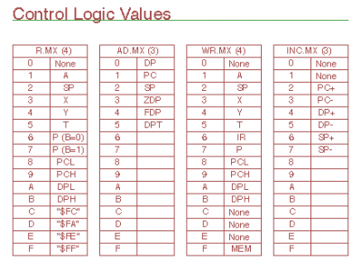
The control circuitry is driven by two Control ROMs. Each ROM is addressed by a 3-bit “Q” state, the current 8-bit Opcode and an INT control flag. Each of the 256 possible opcodes therefore has up to 8 micro-instructions (Q values 0 to 7). The output from these ROMs is decoded to produce all the control signals according to the following table:
Attachment:
control table.png
control table.png [ 14.23 KiB | Viewed 3208 times ]

  • R.MX (4 bits) selects the register to read from and various constants on the R bus. The P register can be read either with a “0” or “1” in the “B” flag.
  • AD.MX selects the address register being used to drive ADL/ADH: DP, PC, SP ($01/SP), ZDP ($00/DPL), FDP ($FF/DPL), and DPT (DPH/T).
  • WR.MX (4 bits) selects the register to write to. $F selects external memory (decoded as "MEM.W").
  • INC.MX controls the INC16 circuit and selects which register will receive the result.
  • IR.LD and DPH.LD are taken directly from the control ROMs without decoding

Each set of MX signals has an associated decoder to break out individual control lines and apply further logic where needed. R.MX and AD.MX produce "R" and "AD" signals as follows:
Attachment:
RMX.png
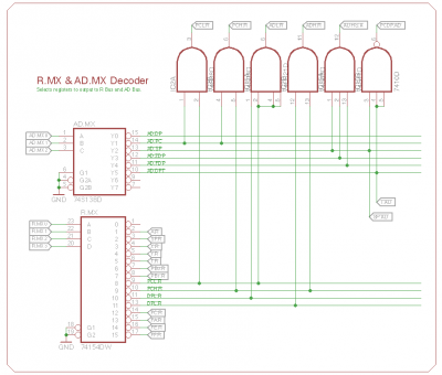
RMX.png [ 41.18 KiB | Viewed 3208 times ]

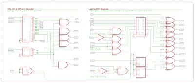
WR.MX and INC.MX are decoded into register-write signals (W signals) which need to be latched by WR.LATCH at the leading edge of phase 2 to prevent glitches and are further gated by /CLK to latch all registers with the trailing edge of phase 2. The memory write signal MEM.W, on the other hand, is clocked to take RW low for the duration of phase 2. PC.SW and DP.SW go to muxes and are left unlatched.
Attachment:
wrmx.png
wrmx.png [ 94.36 KiB | Viewed 3208 times ]

Some logic on the input to WR.LATCH deals with “parallel load” signals (IR.LD and DPH.LD) as well as the INHPF control signal coming from the ALU & CU card (“Inhibit Pre-Fetch” which prevents writing to the PC register and is needed during interrupt handling - more on that later).

Finally, there is also a 96 pin connector. My plan is to put this schematic on one “Registers” card connected to a backplane. I will need at least a second card for the ALU & CU, a third for memory and I/O and a final one for video.

Ok, that pretty much covers it. Now for some questions:

  • Any tips to improve the schematics?
  • Are there any obvious electrical problems evident, either with on-board or backplane connections?
  • Are there more efficient ways to deal with the various addressing requirements (PC, DP, SP, ZDP, etc.)?
  • I could use a wider control word and eliminate the MX decoding logic entirely. There are clear speed advantages to that, but as it stands, I am using 16 bits to encode 38 control signals. Any thoughts or suggestions with respect to this arrangement?
  • I have left the busses active as Garth had suggested, using /BE to tri-state them under external control. Any issues now?
  • I am using Schmitt-trigger gates for the clock signal. All other signals are taken from 96-pin header directly . Is that ok? Should off-board signals be buffered in some way?

Ok, that’s it for now. Many thanks to all for your comments and suggestions.
Best,
Drass


Attachments:
Card A-Registers.png
Card A-Registers.png [ 312.22 KiB | Viewed 3208 times ]

_________________
C74-6502 Website: https://c74project.com
Top
 Profile  
Reply with quote  
 Post subject: Re: TTL 6502 Here I come
PostPosted: Sun Nov 01, 2015 10:32 pm 
Offline
User avatar

Joined: Fri Dec 11, 2009 3:50 pm
Posts: 3346
Location: Ontario, Canada
Thanks for the detailed info, Drass. I haven't yet had a close look but one little improvement did jump out at me. If it works it'll slightly reduce the package count.

In Card A-Registers.png the signal called INT causes $00 to replace the opcode applied to OP[0:7]. If a 74xx273 replaced the '574 (both are octal edge-triggered registers) then the '541 at the bottom of the excerpt below would no longer be required. '273 features an asynchronous Clear input, so that'll give you the $00 when you need it. But there's less tolerance for glitches on INT because the Clear is irreversible, so that needs consideration.

There may be other changes like this that'll reduce package count. But, now that I see what you're doing, it doesn't seem those bidirectional switches would be of much use!

BTW I wonder whether microcode changes might be all that's required to support new instructions of your own creation. I know your initial plan is for undefined opcodes to be NOPs but maybe later you could revisit that... 8)

-- Jeff
Attachment:
IRQ-BRK.gif
IRQ-BRK.gif [ 9.9 KiB | Viewed 3176 times ]

_________________
In 1988 my 65C02 got six new registers and 44 new full-speed instructions!
https://laughtonelectronics.com/Arcana/ ... mmary.html


Top
 Profile  
Reply with quote  
 Post subject: Re: TTL 6502 Here I come
PostPosted: Mon Nov 02, 2015 12:22 am 
Offline
User avatar

Joined: Sun Oct 18, 2015 11:02 pm
Posts: 428
Location: Toronto, ON
Great suggestion Jeff! I'm just not familiar enough with the 7400 chips and these kinds of subtleties elude me. Really appreciate you taking the time to have a look. Thank you!

I was briefly tempted to rework the data path and implement bi-directional buses, but I came to my senses and decided to press on with the current design. That said, I'm intrigued by the notion of attempting to match the 6502 internal structure as closely as possible. I more or less started out with that idea but abandoned it once I realized how crazy a gate-level instruction decoder was going to get. I might be inspired to return to it once I get this version working.

Cheers.

_________________
C74-6502 Website: https://c74project.com


Top
 Profile  
Reply with quote  
Display posts from previous:  Sort by  
Post new topic Reply to topic  [ 558 posts ]  Go to page Previous  1, 2, 3, 4, 5 ... 38  Next

All times are UTC


Who is online

Users browsing this forum: Google [Bot] and 37 guests


You cannot post new topics in this forum
You cannot reply to topics in this forum
You cannot edit your posts in this forum
You cannot delete your posts in this forum
You cannot post attachments in this forum

Search for:
Jump to: