6502.org Forum  Projects  Code  Documents  Tools  Forum
It is currently Sun May 19, 2024 9:35 am

All times are UTC


Post new topic Reply to topic  [ 17 posts ]  Go to page 1, 2  Next
Author Message
PostPosted: Fri Dec 04, 2020 10:54 pm 
Offline

Joined: Fri Dec 04, 2020 8:14 pm
Posts: 8
Hi everyone. Long time lurker, first time poster here.

I've been trying to design a 65C816 computer for a while now and I'm running into some issues that I think go beyond a mistaken connection. I've sent two versions of this computer in for fabrication. The first board didn't work at all. The second board does work, but is unstable under certain conditions. Anyways, I'm starting to think my ideas on the glue logic and address decoding is flawed. For example, if I upload a program to RAM that will never use the EEPROM, it will still activate the EEPROM (briefly). So, running programs within the RAM tends to be unstable.

Here's the link to the full KiCAD project: https://github.com/halfburnttoast/TPC65_V3

For the most part, I'm taking it right from the 65C816's datasheet, using a HC573 and HC245 to latch the bank address. One mistake I did make was to use two 74ALS00's instead of 74HC00's. I don't remember why I went with ALS chips, but I know now that the ALS->HC interface is incompatible and could be a source of the instability.

I've also been cross-referencing my computer with the schematic of WDC's 65C816 SBC and I noticed that they qualified the RAM and ROM's #OE as:
Code:
#OE = !(PHI2 & RWB)

I'm not completely sure why they went this is necessary if #WE overrides the #OE pin during writes, which is what I gathered from the datasheets. But, I'm suspecting that this is also an error on my part. I know I'm also not accounting for VDA and VPA. I'd like to try and include qualification for this by adding a third 74HC00. But, I'm paranoid that I'm overlooking some other aspect of the build.

My proposed memory map looks like:
Code:
0x000000 - 0x007FFF - BANK0 RAM
0x008000 - 0x00BFFF - IO
0x00C000 - 0x00FFFF - EEPROM
0x010000 + N              - remaining banked RAM


To detect BANK0, I'm using a 74F521. But, I'm noticing on the oscilloscope that BANK0 is toggling even when running in emulation mode, which shouldn't happen. The HC573 is briefly latching an invalid value from the databus which, I'm suspecting, is related to it being driven by a ALS00. But, I'm not sure where the primary source of instability is coming from or if it's a constellation of instability.

So, rather than continue burning money on non-working boards, I'd like to see if there are glaring problems with my glue logic. From what I can tell, a lot of people who use the 65C816 use CPLDs as glue logic, but there aren't as many examples of jellybean logic gates, so I've mostly been taking notes from WDC's board. The clock source and serial interface is an Arduino Nano, which I've optimized to put out about a 2.28MHz clock signal. Any help would be appreciated! I can provide more details if needed.

Attachment:
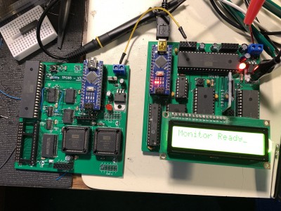
File comment: On right, my working 65C02 design. On left, working but unstable 65C816 board.
2020-12-04_17-23-09_IMG_7244.JPG
2020-12-04_17-23-09_IMG_7244.JPG [ 4.08 MiB | Viewed 1124 times ]


Last edited by HalfBurntToast on Fri Dec 04, 2020 11:53 pm, edited 1 time in total.

Top
 Profile  
Reply with quote  
PostPosted: Fri Dec 04, 2020 11:21 pm 
Offline
User avatar

Joined: Fri Aug 30, 2002 1:09 am
Posts: 8440
Location: Southern California
Make sure there is no way to write to RAM when phase 2 is low. Looking at the timing diagrams in the data sheet, you will see that the address lines are not guaranteed to be valid and stable before the R/W goes low; so it is possible to write to unintended addresses. This information is in the 6502 primer which is about building your own 6502 computer but has a lot of pages that apply equally as well to computers using other processors.

Forgive me if you've already taken care of this; but I can't find the glue-logic info in the github pages (which is usual—I can never find what I want in github!).

_________________
http://WilsonMinesCo.com/ lots of 6502 resources
The "second front page" is http://wilsonminesco.com/links.html .
What's an additional VIA among friends, anyhow?


Top
 Profile  
Reply with quote  
PostPosted: Fri Dec 04, 2020 11:42 pm 
Offline

Joined: Fri Dec 04, 2020 8:14 pm
Posts: 8
GARTHWILSON wrote:
Make sure there is no way to write to RAM when phase 2 is low. Looking at the timing diagrams in the data sheet, you will see that the address lines are not guaranteed to be valid and stable before the R/W goes low; so it is possible to write to unintended addresses. This information is in the 6502 primer which is about building your own 6502 computer but has a lot of pages that apply equally as well to computers using other processors.


Currently I have RW qualified as
Code:
RW_PH2 = !(PH2 & !(RW))

I included it in the screenshots below.

GARTHWILSON wrote:
Forgive me if you've already taken care of this; but I can't find the glue-logic info in the github pages (which is usual—I can never find what I want in github!).

Ah, yeah sorry my schematic needs a bit of tidying up. I've attached images of the bank logic, address decoding, and RW qualification below.

On the image in my first post, the board on the right is my working 65C02 computer and the left is the working-but-unstable 65C816 which matches the schematics currently in the GitHub.


Attachments:
schematic.pdf [293.56 KiB]
Downloaded 44 times
address_decode.png
address_decode.png [ 15.81 KiB | Viewed 1121 times ]
bank_and_rw.png
bank_and_rw.png [ 21.55 KiB | Viewed 1121 times ]
Top
 Profile  
Reply with quote  
PostPosted: Sat Dec 05, 2020 1:04 am 
Offline
User avatar

Joined: Fri Aug 30, 2002 1:09 am
Posts: 8440
Location: Southern California
What's the total gate delay from A16...23 to the RAM and IO chip enables? It looks awfully long; but if you're really running only 2.28MHz, the processor's maximum tADS of 30ns plus the VIA's tACR of 10ns should leave you with 180ns for that long chain of glue logic, which should be totally fine.

Quote:
GARTHWILSON wrote:
Forgive me if you've already taken care of this; but I can't find the glue-logic info in the github pages (which is usual—I can never find what I want in github!).

Ah, yeah sorry my schematic needs a bit of tidying up.

The only apparent schematics I found were some kind of text files which I guess is how KiCAD stores schematics, and I don't have KiCAD, so I never saw any images.

Quote:
I've attached images of the bank logic, address decoding, and RW qualification below.

Thanks. That helps.

_________________
http://WilsonMinesCo.com/ lots of 6502 resources
The "second front page" is http://wilsonminesco.com/links.html .
What's an additional VIA among friends, anyhow?


Top
 Profile  
Reply with quote  
PostPosted: Sat Dec 05, 2020 1:16 am 
Offline

Joined: Mon May 21, 2018 8:09 pm
Posts: 1462
I'll repost here my 3, 4, and 5-chip glue logic examples for '816 systems. They haven't been battle tested, but they do follow sound principles and should work, at least at modest clock speeds (and probably faster ones too, if 74HC is substituted for a faster family). Feel free to substitute your own address decoding, but pay attention to the principles embodied.

The 3-chip design is really minimal, incorporating only the bank address latch additionally to a minimal 65C02 glue logic. A quad 2-NAND generates /OE, /WE, Phi0+2, and the bank latch trigger (Phi1) from the master oscillator. Note carefully that Phi0 (input to the CPU) and Phi2 (to qualify the R/W signals) are one gate delayed from Phi1 - this matches the reaction time delay of the latch itself, so the latter closes its input before the CPU has time to change them (on write cycles, where address integrity is of greatest importance). The third chip is the simplest decoding that puts both ROM and RAM in the appropriate parts of Bank 0; I/O devices are expected to be mapped to a high bank.

The 4-chip design adds a quad 2-NOR to handle RDY, VDA and VPA correctly. Note that Phi0 and Phi2 are now distinct signals, the latter (and Phi1) being qualified by RDY. VDA and VPA are simply used to gate the address decoder, which is otherwise identical to the above. Memory and I/O devices normally ignore /OE and /WE (and adopt their lowest power mode) when their /CE is deasserted.

The 5-chip design changes the decoder so that Bank 0 becomes entirely RAM when the CPU switches to Native mode (ie. the E signal output goes low) but is still half ROM when in Emulation mode, which the '816 boots up in. The glue logic remains the same.

Note that none of the above include a bus transceiver. You only need one of those to isolate the bank address (driven from the CPU during Phi1) from devices that use Phi1 for DMA on the same bus (eg. the traditional CRTC setup). DMA is an advanced topic that you probably shouldn't tackle until you have a basic non-DMA system running reliably.

I strongly prefer to put I/O in a high bank rather than Bank 0. This greatly reduces the need to treat Bank 0 specially on decode, and also reduces address space pressure on the only bank that can contain Direct Page, the CPU stack, and the interrupt vectors. Bank $FF can be identified using a 74HC30 (8-NAND), or any single bank can be identified using a 74HC688 (8-bit equality comparator) - so you don't have to resort to old TTL devices from the 74F family, which may have compatibility problems with devices expecting CMOS input levels.


Attachments:
minimus-glue.png
minimus-glue.png [ 401.25 KiB | Viewed 1103 times ]
Top
 Profile  
Reply with quote  
PostPosted: Sat Dec 05, 2020 1:22 am 
Offline

Joined: Fri Dec 04, 2020 8:14 pm
Posts: 8
GARTHWILSON wrote:
What's the total gate delay from A16...23 to the RAM and IO chip enables? It looks awfully long; but if you're really running only 2.28MHz, the processor's maximum tADS of 30ns plus the VIA's tACR of 10ns should leave you with 180ns for that long chain of glue logic


Yeah, that is something I should probably check going forward. With my particular setup, the computer needs to run synchronously to the Arduino. 2.28MHz is as fast as I can make the Arduino go without losing any of the auxiliary functionality (serial, RNG, etc).

So far I've only tested the computer in emulation mode, which if my understanding is right, should leave BANK0 low permanently as the 65C816 should just send out 0 as the bank address. But, the 74HC573 briefly latches an invalid value which causes the 74F521 to briefly switch BANK0 to high.

GARTHWILSON wrote:
which should be totally fine.


Do you think there's an issue tying the #CE and #OE pins together like I've done? Or should I try and qualify it like WDC did? I suppose I'm not understanding why WDC is qualifying #OE against PHI2, but their schematic is a bit hard to follow.

I've included the full schematic as a PDF here:


Attachments:
File comment: Full schematic
schematic.pdf [293.56 KiB]
Downloaded 61 times
Top
 Profile  
Reply with quote  
PostPosted: Sat Dec 05, 2020 1:36 am 
Offline

Joined: Mon May 21, 2018 8:09 pm
Posts: 1462
You have Phi1 (to the bank address latch) delayed one gate from Phi2, and the latch itself takes about another gate delay to actually close its inputs. One gate in 74HC is about 15ns, which is actually longer than the W65C816S' bank address hold time after the Phi2 rising edge (10ns) - and you have two gate delays in series to worry about here.

So you have approximately 20ns of timing violation during write cycles, and possibly at other times. That could easily explain the latch getting the wrong value occasionally. See my glue logic examples above for a better way to handle this.


Top
 Profile  
Reply with quote  
PostPosted: Sat Dec 05, 2020 1:37 am 
Offline

Joined: Fri Dec 04, 2020 8:14 pm
Posts: 8
Chromatix wrote:
I'll repost here my 3, 4, and 5-chip glue logic examples for '816 systems.


Wow, thanks for posting that. I'll need to study it when I'm not so tired :mrgreen: .

Pretty much, I was following WDC's design straight out of the datasheet. Now that you mention it, the bus transceiver makes more sense now (and possibly WDC's #OE qualification). Guess DMA never crossed my mind, I was more interested in getting a working system.

The main reason I'm keeping the memory map like that is it's the same as the 65C02 computer I made. I wanted it to be fully backwards compatible with the computer next to it. To the point where I was just literally taking the ROM chip out of one and putting it into the 816's socket and running it. It does run, it just has this latent instability that's a real thorn to track down.

Specifically, when I load my homebrew version of Forth into RAM and run it, it becomes very unstable and eventually crashes. I know something's up as it runs perfectly fine on the 65C02 machine. My suspicion is the 74ALS00 chips as a large factor, but I'm paranoid I've made some other logic error.


Top
 Profile  
Reply with quote  
PostPosted: Sat Dec 05, 2020 1:45 am 
Offline

Joined: Fri Dec 04, 2020 8:14 pm
Posts: 8
Chromatix wrote:
You have Phi1 (to the bank address latch) delayed one gate from Phi2, and the latch itself takes about another gate delay to actually close its inputs.


Huh... well shoot. That gating was actually something I tried to copy from WDC's SBC exactly as-is. I figured it would work without looking much into it.

But, I've read on here that design isn't the greatest either.


Attachments:
wdc.png
wdc.png [ 43.61 KiB | Viewed 1100 times ]
Top
 Profile  
Reply with quote  
PostPosted: Sat Dec 05, 2020 1:52 am 
Offline

Joined: Mon May 21, 2018 8:09 pm
Posts: 1462
Alas, WDC documentation is known to contain random errors, and one of their commercially sold reference SBCs was recently found to use a CD4000-series chip that didn't have a hope of meeting timing at the stock clock speed, but worked okay as long as you never left Bank 0.

After deciding that the logic shown in the '816 datasheet was worthless for novice SBC builders, I worked out the above from first principles. I really should get some parts and try it out for real…


Top
 Profile  
Reply with quote  
PostPosted: Sun Dec 06, 2020 10:42 pm 
Offline

Joined: Fri Dec 04, 2020 8:14 pm
Posts: 8
Chromatix wrote:
one of their commercially sold reference SBCs was recently found to use a CD4000-series


Oof. That's pretty discouraging.

Thanks again for posting your timing examples. I think I get what you're going for. I took some time to play around with different setups and I've come up with a new layout based on what you said and what I saw on a couple other sites.

In this version, I'm dropping the banked address entirely, partly because the chip I wanted is on backorder, but also I'm more concerned about getting a basic, working build. This uses exactly the same address decoding scheme as my 65C02 build and should be completely backwards compatible (again, to remove things that can go wrong). And I know my 65C02 build is stable until about 12MHz, even though it will only be running 2.28MHz.

I still probably need to factor in VPA and VDA, but do you see any issues that I might have missed with this layout? The only thing that comes to mind, for me, is I'll probably need to reverse the clock generation code on the Arduino to account for the inverted PH0 to the CPU.


Attachments:
schem_bw.pdf [126.64 KiB]
Downloaded 46 times
logic.png
logic.png [ 14.22 KiB | Viewed 1046 times ]
Top
 Profile  
Reply with quote  
PostPosted: Sun Dec 06, 2020 11:35 pm 
Offline

Joined: Mon May 21, 2018 8:09 pm
Posts: 1462
Yes, I think that looks correct for a basic 65C02-style glue and decode, and should work fine with an '816.

The one thing you could take advantage of is to feed VDA into one side of the NAND you're using for the R/W inverter, so that it qualifies all write cycles (which will always be data cycles). You could do the same with /IO_CE if you had a 3-NAND there instead of a 2-NAND; you should expect that all I/O access cycles will be data cycles. Since the RAM and ROM don't care about spurious reads (except for consuming a little power unnecessarily), that ensures that all cycles will be safe.

That extra qualification is entirely optional though, as the '816 always pulls R/W high and drives a "safe" address for "internal operation" cycles.

I do have to ask, though, why your connection to the Arduino doesn't have either the R/W or the /OE and /WE lines connected? How does it know what type of cycle is intended?


Top
 Profile  
Reply with quote  
PostPosted: Mon Dec 07, 2020 12:07 am 
Offline
User avatar

Joined: Thu May 28, 2009 9:46 pm
Posts: 8190
Location: Midwestern USA
Chromatix wrote:
The one thing you could take advantage of is to feed VDA into one side of the NAND you're using for the R/W inverter...

I disagree with that. Reads and writes should be qualified with Ø2 and VDA/VPA should be used to qualify device selection per WDC recommendations.

Quote:
That extra qualification is entirely optional though, as the '816 always...drives a "safe" address for "internal operation" cycles.

There is nothing in the documentation that supports that claim. In fact, WDC states on page 15 of the data sheet that when VDA OR VPA is false the "...Address Bus may be invalid." They essentially repeat this on page 50: "Note that when VDA and VPA are both low, invalid addresses may be generated. The Page and Bank addresses could also be invalid."

_________________
x86?  We ain't got no x86.  We don't NEED no stinking x86!


Top
 Profile  
Reply with quote  
PostPosted: Mon Dec 07, 2020 12:21 am 
Offline

Joined: Mon May 21, 2018 8:09 pm
Posts: 1462
The datasheet does actually specify in Table 5-7, for each instruction group and addressing mode, what addresses appear on the bus during IO (internal operation) cycles. In most cases they are either re-reads of the immediately previously read address, or a spurious fetch from the next program address in sequence. The only exception is for certain indexed addressing modes, where a fetch from an incompletely calculated address may occur.

In all these cases, VDA will be low and can be used to suppress I/O space accesses, as I/O devices are most likely to be adversely affected by spurious reads, and VPA will never be high for a valid I/O space access. But you can also avoid the ill effects in the same way as on the 65C02, which doesn't have a VDA signal with which to do so.


Top
 Profile  
Reply with quote  
PostPosted: Mon Dec 07, 2020 12:35 am 
Offline

Joined: Fri Dec 04, 2020 8:14 pm
Posts: 8
Chromatix wrote:
I do have to ask, though, why your connection to the Arduino doesn't have either the R/W or the /OE and /WE lines connected? How does it know what type of cycle is intended?


Heh, the entire system with the Arduino is a pretty hacky. But, somehow does work. It uses the three address lines and #IO_CE to determine if the computer is looking for some function from the Arduino. The Arduino is in full control of the clock, so it pauses the outgoing clock signal if it's being accessed and does whatever function the machine is looking for. Otherwise it ignores the input.

The operation does seem to rely on a race-condition, though. The logical process for a write ends up being:
[*] Clock pulse
[*] Check address pins
[*] Set bus lines to output
[*] Write data value
[*] Set bus lines to input
[*] Clock pulse

So, the pins are floating during that time. Which you'd think would be a problem, but every computer build I've tested it on with a 65C02 runs stable. Transferring files through the monitor hasn't had any problems.

Making this process cleaner is on my to-do list. The 65C816 build, while unstable, doesn't seem to have an issue with this setup either.

This is the code. It's a bit of a mess with header switches.
https://github.com/halfburnttoast/nano_6502_controller/blob/master/nano_6502_controller.ino


Top
 Profile  
Reply with quote  
Display posts from previous:  Sort by  
Post new topic Reply to topic  [ 17 posts ]  Go to page 1, 2  Next

All times are UTC


Who is online

Users browsing this forum: No registered users and 1 guest


You cannot post new topics in this forum
You cannot reply to topics in this forum
You cannot edit your posts in this forum
You cannot delete your posts in this forum
You cannot post attachments in this forum

Search for:
Jump to: