6502.org Forum  Projects  Code  Documents  Tools  Forum
It is currently Sun Jun 30, 2024 1:26 pm

All times are UTC


Post new topic Reply to topic  [ 9 posts ] 
Author Message
PostPosted: Mon Jan 28, 2013 10:08 pm 
Offline

Joined: Mon Jan 28, 2013 3:09 am
Posts: 35
I'm trying to understand the clock signals of the 6502 and how they run in the visual simulator:http://visual6502.org/JSSim/expert.html

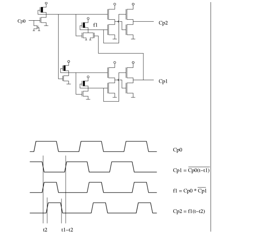
In the simulator I managed to figure out the following nodes:
cclk, cp1, clk0

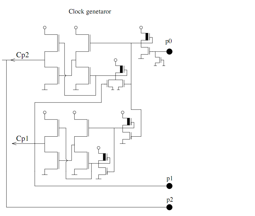
In the following schematic I see there is a clock generator which has
p0, p1, p2, Cp1, Cp2

Image

This is part of the schematic that can be obtained from http://www.downloads.reactivemicro.com/Public/Electronics/CPU/.

Lastly, I hear people talking about phi1 and phi2 all the time. Is that the same as phase1 and phase2?

So my questions are:

1. How are cclk, cp1, clk0; p0, p1, p2, Cp1 Cp2; phi1 and phi2 related?
2. Where on the visual simulator is the clock generator located as detailed in the schematic? Notice that the schematic is turned 180° in relation to the visual simulator. I suspect the location is on the top almost at the right corner.


Last edited by cerebrum on Tue Jan 29, 2013 8:26 pm, edited 2 times in total.

Top
 Profile  
Reply with quote  
PostPosted: Mon Jan 28, 2013 11:15 pm 
Offline
User avatar

Joined: Thu Dec 11, 2008 1:28 pm
Posts: 10837
Location: England
Hi Cerebrum, and welcome!

Yes indeed, phi1 and phase1 are the same things. Sometimes people use the Greek Phi character: Φ and φ for uppercase and lowercase respectively.

On the top edge of the 6502, as viewed in visual6502, you'll find the third pad from the right is clk0 which would be bonded to the phi0 clock input pin (and next to it the pad for cclk which is not connected for 6502 but is (surely) the direct input of the phase2 on-chip clock in the 6501.) This phi0 pin is marked as p0 in your schematic extract.

http://visual6502.org/JSSim/expert.html?find=clk0

Most of the clocking on the chip is done by two signals: called cp1 and cclk in visual6502. cp1 is phase 1 and cclk is phase 2. Visual6502 simulates only at the clock phase level of granularity, so it can't show the small delays between the successive stages of buffers or inverters. As your schematic extract shows, the phi2 drive circuit uses a NOR gate to ensure that it's low when phi1 is high.

Disregarding small delays, we have just two phases with several names:
phi0 AKA clk0 AKA p0, all same phase as phi2 AKA cclk AKA cp2 AKA p2
phi1, cp1 AKA p1.

Note that nodes 43 and 1247 which control some of the datapath control signals are also directly derived from cp1, so they are somewhat like phi2 but with some difference in timing.

Hope this helps
Ed


Top
 Profile  
Reply with quote  
PostPosted: Tue Jan 29, 2013 12:18 am 
Offline

Joined: Mon Jan 28, 2013 3:09 am
Posts: 35
BigEd wrote:
Disregarding small delays, we have just two phases with several names:
phi0 AKA clk0 AKA p0, all same phase as phi2 AKA cclk AKA cp2 AKA p2
phi1, cp1 AKA p1.


Hi Ed,

thanks for the warm welcome!

I've a diagram with the clock phases:
Image

Which is from the beginning of this pdf:

http://www.downloads.reactivemicro.com/Public/Electronics/Reverse%20Engineering/6502%20-%20Integration.pdf

So are those waves correct representations of Cp0, Cp1 and Cp2? Notice that Cp2 has not only a small delay but the "up" portion is also shorter.


Last edited by cerebrum on Tue Jan 29, 2013 3:46 am, edited 1 time in total.

Top
 Profile  
Reply with quote  
PostPosted: Tue Jan 29, 2013 12:30 am 
Offline

Joined: Mon Jan 28, 2013 3:09 am
Posts: 35
Ed,

could you please pinpoint where exactly on the visual chip the clock generator circuit is located? Is it to the left of the clk0 pad, encompassing the area until the so pad?

http://visual6502.org/JSSim/expert.html


Last edited by cerebrum on Tue Jan 29, 2013 12:41 am, edited 1 time in total.

Top
 Profile  
Reply with quote  
PostPosted: Tue Jan 29, 2013 12:39 am 
Offline

Joined: Mon Jan 28, 2013 3:09 am
Posts: 35
BigEd wrote:
On the top edge of the 6502, as viewed in visual6502, you'll find the third pad from the right is clk0 which would be bonded to the phi0 clock input pin (and next to it the pad for cclk which is not connected for 6502 but is (surely) the direct input of the phase2 on-chip clock in the 6501.) This phi0 pin is marked as p0 in your schematic extract.


This clk0 aka phi0, p0 pad, does it receive a clock signal from outside the 6502? So the clock is not inside the 6502 but an outside component on the motherboard, right? The other phases phi1 and phi2 are then generated internally from the phi0 by the clock generator circuit, correct?


Top
 Profile  
Reply with quote  
PostPosted: Tue Jan 29, 2013 8:37 am 
Offline
User avatar

Joined: Thu Dec 11, 2008 1:28 pm
Posts: 10837
Location: England
Hi Cerebrum
quick answers as I have to go to work:
- yes, I'm sure that wave diagram is good. When I say 'same phase' I mean only broadly similar to phi1 or phi2: any inverter or buffer will add a small phase shift, as as noted, NOR gates or similar will affect the leading or trailing edge depending on what they are doing.
- yes, the clock driver circuit is to the left of the pad, and runs almost as far as the SO pin.
- yes, phi0 is the (single) input clock from outside the 6502, and everything else is generated onchip. This was one of the big innovations compared to previous chips: the 6800 and the pin-compatible short-lived 6501 used off-chip clock generators. The off-chip circuit solved the problems of:
- non-overlapping
- full-rail swings
- large drive
and this was necessary for 6800 because the on-chip technology could not produce a full-rail swing with large drive in an acceptable way. The MOS company used depletion transistors (as did the later 6809) on-chip, which does allow for full-rail drive.

If the clocks on a chip are not full-rail, then it's very difficult to use pass transistor circuits, which are very compact and efficient. An alternative is to have several supply voltages, which is what the 8080 did.

Cheers
Ed


Top
 Profile  
Reply with quote  
PostPosted: Tue Jan 29, 2013 8:15 pm 
Offline

Joined: Mon Jan 28, 2013 3:09 am
Posts: 35
Thanks Ed!


Top
 Profile  
Reply with quote  
PostPosted: Tue Jan 29, 2013 8:56 pm 
Offline

Joined: Mon Jan 28, 2013 3:09 am
Posts: 35
I just noticed that to the left of the "so" pad there is a clk2out pad. I assume this is phi2 also, correct?


Top
 Profile  
Reply with quote  
PostPosted: Tue Jan 29, 2013 9:28 pm 
Offline
User avatar

Joined: Thu Dec 11, 2008 1:28 pm
Posts: 10837
Location: England
Yes. Interestingly, clk2out is derived from clk0 (input pad) combined with cp1 (on-chip phi1), and similarly the inverted clk0 used for clk2out is taken to the clk1out pad.

It might be amusing to trace all these clock signals (internal and external) in a spice simulation, putting some typical load on the output pads. See viewtopic.php?p=13550#p13550


Top
 Profile  
Reply with quote  
Display posts from previous:  Sort by  
Post new topic Reply to topic  [ 9 posts ] 

All times are UTC


Who is online

Users browsing this forum: No registered users and 2 guests


You cannot post new topics in this forum
You cannot reply to topics in this forum
You cannot edit your posts in this forum
You cannot delete your posts in this forum
You cannot post attachments in this forum

Search for:
Jump to: