6502 + at28c256 always reading wrong data
Posted: Sun Mar 14, 2021 6:42 pm
I've been struggling with this problem for 3 weeks now and have run out of ideas on how to troubleshoot this. Hoping someone here might be able to point me in the right direction.
I've got a WDC 65c02 paired with an AT28C256 EEPROM that I've programmed entirely with $ea as a means of testing. I'm using a TL866ii+ and I've written/read from the 3 different EEPROMs using both the OEM Windows software and David Griffith's "minipro" software. The chips all check out ok - the reads and writes are successful.
The problem, however, is that once the EEPROM is in my circuit, the 6502 always reads $fffc as $00. Each of the three AT28C256's behave the same.
$fffd reads properly as $ea, thus my starting address is always $ea00 instead of $eaea.
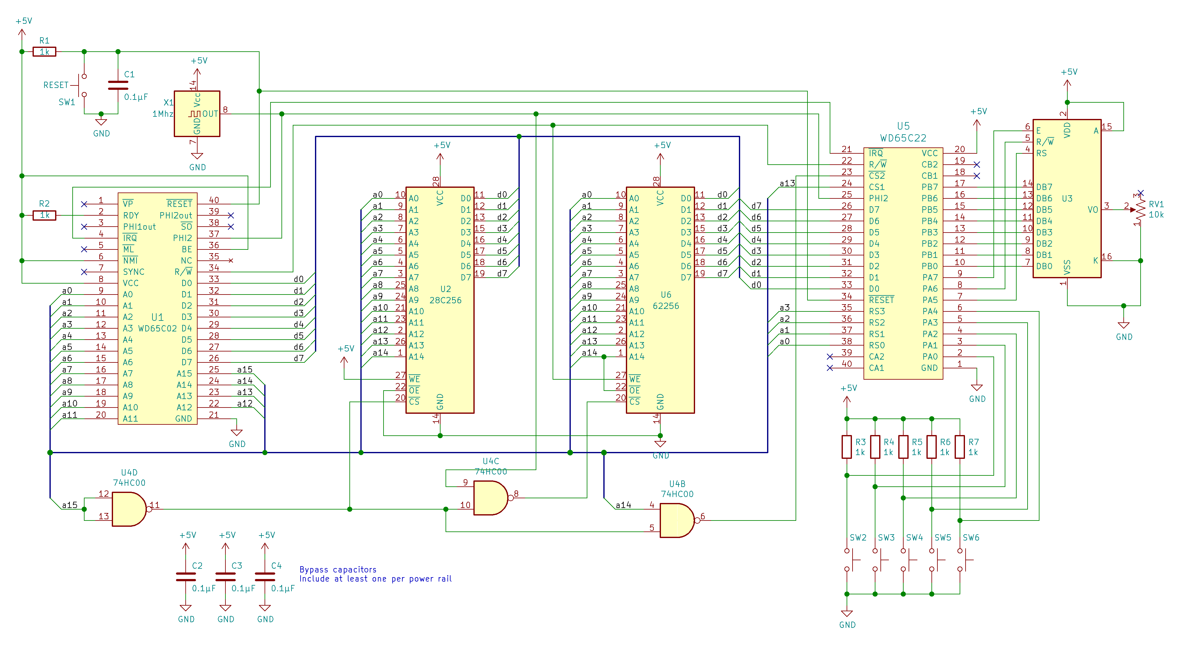
The clock is manual right now and based on 555 timers - built following Ben Eater's project on YouTube.
Monitoring the address and data pins with an Arduino, the output below is consistent. I have disassembled and rebuilt the circuit 3 times, double/triple checking my wiring, components, continuity, and voltages.
r/W is output from pin 34 (RWB), last two characters is the data read in.
With the EEPROM programmed for all $ea ... I'm only expecting the 6502 to go to $eaea after initialization and proceed counting up from that address with a series of NOP instructions.
I've also replaced the 65c02 thinking perhaps my chip was the culprit - but same behavior on the other 65c02 as well.
Someone had suggested I try programming the EEPROMs with something other than $ea - and since it always wants to jump to $ea00, put the instructions there. I've done this, but unfortunately I'm still quite early in learning about the 6502 and I'm not able to make much sense of this.
I programmed one of the AT28C256's with the following:
When run in the circuit, this was the result:
By this point I had detatched the Arduino from the address pins thinking maybe a problem with the Arduino could be causing timing issues. This is why all of the addresses show as "0000" in the output above. But notice how the execution never makes it all the way through my instructions - so I believe the problem is manifesting itself here as well.
Basically I'm completely stuck at the moment an unsure what to troubleshoot next. Any suggestions on something I can try?
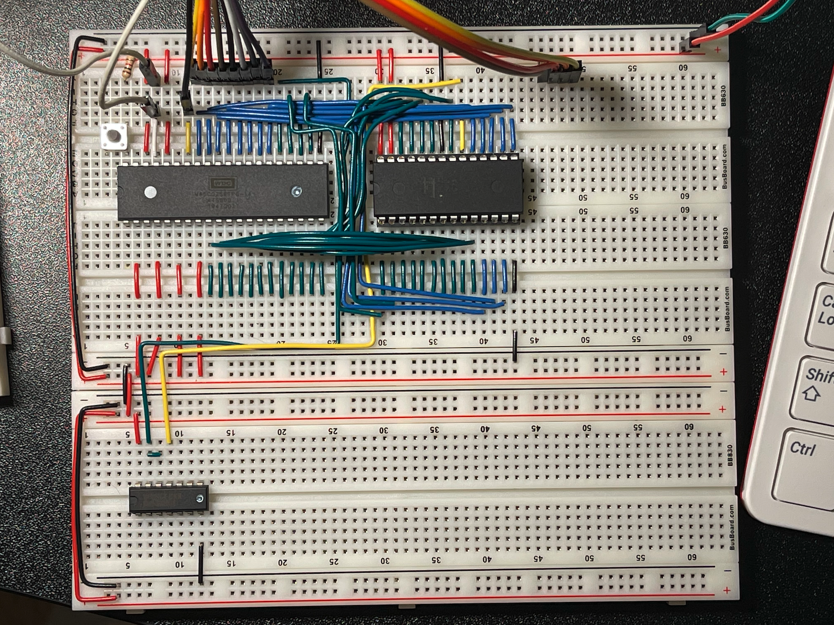
Pic of my circuit can be found here: https://imgur.com/a/V4fHCDu
I've got a WDC 65c02 paired with an AT28C256 EEPROM that I've programmed entirely with $ea as a means of testing. I'm using a TL866ii+ and I've written/read from the 3 different EEPROMs using both the OEM Windows software and David Griffith's "minipro" software. The chips all check out ok - the reads and writes are successful.
The problem, however, is that once the EEPROM is in my circuit, the 6502 always reads $fffc as $00. Each of the three AT28C256's behave the same.
$fffd reads properly as $ea, thus my starting address is always $ea00 instead of $eaea.
The clock is manual right now and based on 555 timers - built following Ben Eater's project on YouTube.
Monitoring the address and data pins with an Arduino, the output below is consistent. I have disassembled and rebuilt the circuit 3 times, double/triple checking my wiring, components, continuity, and voltages.
Code: Select all
|-address pins-| |data pins|
1111111111111111   11101010   ffff  r ea
1111111111111111   11101010   ffff  r ea
1111111111111111   11101010   ffff  r ea
0000000000000000   11101010   0000  r ea
0000000100000000   11101010   0100  r ea
0000000111111111   11101010   01ff  r ea
0000000111111110   11101010   01fe  r ea
1111111111111100   00000000   fffc  r 00
1111111111111101   11101010   fffd  r ea
1110101000000000   00000000   ea00  r 00
1110101000000001   11101010   ea01  r ea
0000000111111101   11101010   01fd  W ea
0000000111111100   00000010   01fc  W 02
0000000111111011   00110100   01fb  W 34
1111111111111110   00000000   fffe  r 00
1111111111111111   11101010   ffff  r ea
With the EEPROM programmed for all $ea ... I'm only expecting the 6502 to go to $eaea after initialization and proceed counting up from that address with a series of NOP instructions.
I've also replaced the 65c02 thinking perhaps my chip was the culprit - but same behavior on the other 65c02 as well.
Someone had suggested I try programming the EEPROMs with something other than $ea - and since it always wants to jump to $ea00, put the instructions there. I've done this, but unfortunately I'm still quite early in learning about the 6502 and I'm not able to make much sense of this.
I programmed one of the AT28C256's with the following:
Code: Select all
rom[0x6a00] = 0x08
rom[0x6a01] = 0x18
rom[0x6a02] = 0x28
rom[0x6a03] = 0x38
rom[0x6a04] = 0x48
rom[0x6a05] = 0x58
rom[0x6a06] = 0x68
rom[0x6a07] = 0x78
rom[0x6a08] = 0x88
rom[0x6a09] = 0x98
rom[0x6a0a] = 0xa8
rom[0x6a0b] = 0xb8
rom[0x6a0c] = 0xc8
rom[0x6a0d] = 0xd8
rom[0x6a0e] = 0xe8
rom[0x6a0f] = 0xf8

rom[0x6a10] = 0x20
rom[0x6a11] = 0x00
rom[0x6a12] = 0xea
Code: Select all
   11101010   0000  r ea
   11101010   0000  r ea
   11101010   0000  r ea
   11101010   0000  r ea
   11101010   0000  r ea
   11101010   0000  r ea
   00000000   0000  r 00  <- $fffc
   11101010   0000  r ea
   00001000   0000  r 08  <- $ea00 ($6a00 on the eeprom)
   00011000   0000  r 18  <- $ea01 ($6a01)
   00110100   0000  W 34
   00000000   0000  r 00
   00101000   0000  r 28  <- $ea02 ($6a02)
   11101010   0000  W ea
   00000011   0000  W 03
   00110100   0000  W 34
   00000000   0000  r 00
   11101010   0000  r ea
   00001000   0000  r 08  <- back to $ea00 and repeat
   00011000   0000  r 18
   00110100   0000  W 34
   00000000   0000  r 00
   00101000   0000  r 28
   11101010   0000  W ea
   00000011   0000  W 03
   00110100   0000  W 34
   00000000   0000  r 00
   11101010   0000  r ea
   00001000   0000  r 08  <- cycle starts again
   00011000   0000  r 18
   00110100   0000  W 34
   00000000   0000  r 00
   00101000   0000  r 28
   11101010   0000  W ea
   00000011   0000  W 03
   00110100   0000  W 34
   00000000   0000  r 00
   11101010   0000  r ea
Basically I'm completely stuck at the moment an unsure what to troubleshoot next. Any suggestions on something I can try?
Pic of my circuit can be found here: https://imgur.com/a/V4fHCDu